
Last Updated on October 22, 2023 by Kevin Chen
Image source Amazon
One of the popular members in the 74XXXYY IC series is the 74LS00 NAND Gate. Like most members of this logic gate, it does not operate independently. Instead, it is part of larger circuits that are used for complex tasks and operations. In most cases, it forms part of the integrated circuits (ICs) which is basically a combination of many other smaller electronic components.
Are you planning to buy 74LS00 NAND Gate for your project, or would you like to buy them in bulk? This is a perfect guide for you. We are going to explore everything you need to know about 74LS00 NAND gates.
74LS00 pin configuration
74LS00 NAND is a 14-pin gate and let’s look at the detailed configuration of its pins.
NAND GATE 1
1: A1- Input1 of Gate1
2: B1-Input2 of Gate 1
3: Y1-Output of Gate 1
NAND GATE 2
4: A2 Input1 of Gate2
5:B2 Input2 of Gate 2
6: Y2 Output of Gate 2
NAND GATE 3
9: A3 Input 1 of Gate 3
10: Input 2 of Gate 3
8: Y3 Output of Gate 3
NAND Gate 4
12: A4 Input 1 of Gate 4
13: B4 Input 2 of Gate 4
11: Output of Gate 4
Shared Terminals
7: GND – Ground or connected to ground
14: VCC This pin is connected to the positive voltage power source
All these pins play individual specific roles in the logic operation of the 74LS00 NAND gate.
How 74LS00 NAND gate works?
As we have already seen from the above pin configuration, 74LS00 contains four NAND gates. Each gate has two input pins and one output pin. These pins are labeled as A, B and Y respectively.
Just like any other digital logic gate, 74LS00 NAND is designed to produce an output that is logical of the input circuits. This implies that the two inputs should be AND then inverted hence the NAND. The output of the logic gate will be low only when both inputs are high.
To give you a better understanding, let’s take a look at the Truth table below
| Input 1 | Input 2 | AND output | NAND Output |
| Low (0) | Low (0) | Low (0) | High (1) |
| High (1) | Low (0) | Low (0) | High (1) |
| Low (0) | High (1) | Low (0) | High (1) |
| High (1) | High (1) | High (1) | Low (0) |
Now we should be able to translate the table above to an actual functional circuit. For example, lets say the logic gate is used in transistors. When the two inputs of the transistor are low, it means that the transistor is off hence no current will flow through the output. Given the NAND operation, the overall output will be high.
You want a better explanation? Let’s look at these steps using the image below as a reference
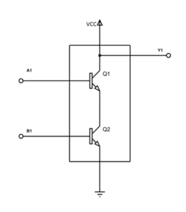
Image source Components 101
Let’s say the inputs A and B of the 74LS00 NAND gate are connected to the transistors Q1 and Q2.
When both logic gate inputs are low (0), the transistors Q1 and Q2 will also be low and this will also mean that the Q3 output from the transistor will be low.
When either input A or B is high, this will trigger the transistor to turn ON and current will flow through the output Q3. Since it serves as an inverter, the output will be low.
Usually, the Q3 will remain at a low state until the inputs get back to the 0 state. This waiting period is known as the propagation delay and lasts for microseconds.
Overall, the working mechanism of a 74LS00 NAND gate entails the implementation of a logic gate in a circuit.
Technical specifications of 74LS00 NAND gate
Here are the key features and specifications of the 74LS00 NAND gate:
- Maximum supply voltage 7V
- VCC supply voltage 4.75
- Maximum input current allowed 8mA
- Operating voltage range 4.75 V- 5.25V
- Operating temperature 0°C to 75°C
- Estimated rise time 15 ns
- Estimated fall time 15 ns
Using the 74LS00 NAND Gate
Now that you know how the 74LS00 NAND gate works, let’s see how it is connected and used in electric circuits. We will take an example of using this gate to control the operation of LED lights as shown in the image below:
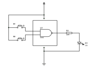
Image source Components101
From the above image, the two inputs of the 74LS00 NAND gate are connected two buttons while the output is connected to an LED light source. With the LED, you will be able to tell when the output is ON and OFF.
Take note of the buttons B1 and B2 that are connected to the input pins. In most cases, they are not pressed meaning that the input gates will be low. From the truth table that we have just discussed, two LOW inputs will result in a HIGH output. This implies that the LED will turn ON.
What if you press one button? Let’s say you close B1. One input will be LOW while the other one will be HIGH. From our truth table, the output will be HIGH hence the bulb will turn ON.
The LED will be off only when both buttons are pressed as we can see from the truth table.
When connecting the 74LS00 NAND gate, you need to know its pinout and configuration. The gate is designed to have a dual in-line pin arrangement whereby each of the two rows has seven pins.
You should also connect it to the right power supply as we have mentioned in the technical specifications.
Applications of 74LS00 NAND gate
When integrated into a circuit, the 74LS00 NAND gate is used to perform the NAND function of the logic gate. For example, you can use it to invert a logic gate.
Common application areas of the NAND include:
- General purpose logic gate
- Networking applications
- Digital circuits
- Computers, PCs and notebooks
- Network servers
Where do you intend to use the 74LS00 NAND gate? Whatever application area that you choose, ensure that you buy quality logic gates from reputable suppliers in China. This rule applies even when buying 74LS00 NAND gates wholesale.
If you want to find more Electronic Components Distributors, please check out the following articles:
Electronic Components Distributors In the USA
Electronic Components Distributors In UK
Electronic Components Distributors In China
Electronic Components Distributors In India
Electronic Components Distributors In Singapore
Electronic Components Distributors In Malaysia
Electronic Components Distributors In Vietnam
Electronic Components Distributors In South Korea
- Where to buy IC chips? The Best Guide? - March 26, 2024
- Breaking Down Barriers: Overcoming Obstacles in Cross-Border Electronic Component Trade - March 4, 2024
- Everything You Need to Know About Amplifier IC Chips - March 4, 2024


