ADC0804LCN
Part Number: ADC0804LCN
Manufacturer: Texas Instruments
Description: IC ADC 8BIT SAR 20DIP
Shipped from: Shenzhen/HK Warehouse
Stock Available: Check with us
ICRFQ.com - Electronic Components Distributor in China Since 2003

We make your sourcing easier!
Get A Fast Quote Worldwide!

Part Number: ADC0804LCN
Manufacturer: Texas Instruments
Description: IC ADC 8BIT SAR 20DIP
Shipped from: Shenzhen/HK Warehouse
Stock Available: Check with us
| Datasheet | |
|---|---|
| Category | Integrated Circuits (ICs) |
| Family | Data Acquisition – Analog to Digital Converters (ADC) |
| Manufacturer | Texas Instruments |
| Series | – |
| Packaging | Tube |
| Part Status | Active |
| Number of Bits | 8 |
| Sampling Rate (Per Second) | 10k |
| Number of Inputs | 1 |
| Input Type | Differential |
| Data Interface | Parallel |
| Configuration | ADC |
| Ratio – S/H:ADC | – |
| Number of A/D Converters | 1 |
| Architecture | SAR |
| Reference Type | External, Supply |
| Voltage – Supply, Analog | 4.5 V ~ 6.3 V |
| Voltage – Supply, Digital | 4.5 V ~ 6.3 V |
| Features | – |
| Operating Temperature | 0°C ~ 70°C |
| Package / Case | 20-DIP (0.300″, 7.62mm) |
| Supplier Device Package | 20-DIP |
The ADC0804 is an 8-bit IC that can simultaneously take readings from up to 8 analog inputs. In other words, the range of the digital output is 0-255. A converter based on the differential potentiometric ladder is used to make successive approximations.
Every device cannot do every operation. Devices that can conduct one set of operations and transform them into a format usable by another group of devices are never in short supply. The primary challenge we confront is the translation of data between various devices.
Most innovations in electronics have resulted from the need for gadgets to communicate effectively with one another so that they can work with two or more distinct items or devices.
The results of any number of past and future occurrences can be expressed mathematically. There is no discrete representation for these mathematical values. In other words, we can state that these numbers always have a beginning and an end but that there is an endless range of possible values.
In the temporal domain, these values are intuitive (real life). Most people aren’t good readers, including machines and other modern gadgets. They might be able to read the beginning or the conclusion, but they usually can’t. The frequency domain is the operational environment for all mechanical and electronic equipment. Typically, A/D Converters are employed to address such problems (ADC).
Several different ADCs are available for digitizing analog signals for microprocessors and controllers. Other “ADCs” have various advantages and features depending on the situation. The low voltage 8-bit analog to Digital Converter, or “ADC0804 IC,” will be discussed in this article.
The ADC0804 is an 8-bit IC designed to convert low-voltage analog signals into digital form. It accepts inputs between 0 and 5 Volts, has single Analog information, and 8 outputs. Even though the ADC0804 has its built-in clock, we can utilize the external clock to increase or decrease the frequency of the clock. Whether using an internal or external clock, we can’t exceed a conversion speed of 110us.
ADC0804, like many other electronic devices, has an internal circuit that is a little complex. The analog-to-digital converter ADC0804 employs a wide variety of logic components—including gates, flip-flops, decoders, shift registers tri-states, latches, clocks, ladders, etc.— to convert analog signals to digital. But the SAR Latch is the primary component of ADC0804 for signal conversion.
Binary searching across all available quantization/mapping levels allows SAR Latch to transform a continuous analog signal into a digital signal/discrete signal. The “ADC0804” also uses other parts to produce the correct output in response to the input. When waiting for a high-to-low pulse, data can be temporarily stored in a tri-state register. The result is serialized using an 8-bit shift register so that it can be read by other devices expecting a binary representation.
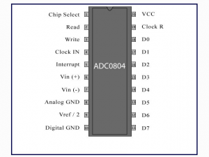
Any time we get an analog value with a Potential Difference between 2.5 and 6.5, we can use an ADC0804. Some requirements must be met before we may use the ADC0804. The Vcc pin will be connected to a 5 V DC power source, and the GND pin will be grounded.
The device can be activated by connecting the ground to the CS pin. Applying ground to the RD and WR pins will make the device readable and writable for data. They connect a 10K resistor and 100pF capacitor to the clock pin, forming the RC circuit necessary for using the internal clock. These specifications are what allow the ADC0804 to function.
An ADC0804 integrated circuit (IC) performs the task of transforming analog voltage input into a digital representation of that value. It can convert analog signals to digital signals on its own. Although revolutionary at the time, modern analog-to-digital converters offer greater versatility, reduced power consumption, output in various formats, and smaller form factors, making the older technology obsolete.
For more details or purchase of ADC0804 integrated circuit (IC), contact us aT ICRFQ. We are the best distributors of IC and electronic components in China.
WhatsApp us