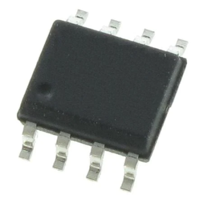
AT45DB321D-SU
Part Number: AT45DB321D-SU
Manufacturer: Adesto Technologies
Description: NOR Flash 32M 2.7-3.6V, 66Mhz Data Flash
Shipped from: Shenzhen/HK Warehouse
Stock Available: Check with us
ICRFQ.com - Electronic Components Distributor in China Since 2003

Part Number: AT45DB321D-SU
Manufacturer: Adesto Technologies
Description: NOR Flash 32M 2.7-3.6V, 66Mhz Data Flash
Shipped from: Shenzhen/HK Warehouse
Stock Available: Check with us
| Datasheet | |
|---|---|
| Category | Integrated Circuits (ICs) |
| Family | Memory |
| Manufacturer | Adesto Technologies |
| Series | – |
| Packaging | Tube |
| Part Status | Obsolete |
| Format – Memory | FLASH |
| Memory Type | DataFLASH |
| Memory Size | 32M (8192 pages x 528 bytes) |
| Speed | 66MHz |
| Interface | SPI, RapidS |
| Voltage – Supply | 2.7 V ~ 3.6 V |
| Operating Temperature | -40°C ~ 85°C (TC) |
| Package / Case | 8-SOIC (0.209″, 5.30mm Width) |
| Supplier Device Package | 8-SOIC |
The AT45DB321D-SU is a 2.3V minimum, serial-interface sequential access Flash memory appropriate for various digital audio, image, and data storage applications. These applications include program code storage. The AT45DB321D-SU supports the RapidS serial interface, which can be used for applications needing very high-speed operation.
Memory is organized in 8,192 pages, each of which contains 512 or 528 bytes, and has a total capacity of 34,603,008 bits. In addition to the primary memory, the AT45DB321D-SU has two SRAM buffers, each storing 512/528 information. The buffers allow data to be received even while a page in the main memory is reprogrammed. When both buffers are interleaved, a system’s capacity to write a continuous data stream can significantly increase. E2PROM emulation (bit or byte alterability) can also be readily handled with a self-contained three-step read-modify-write procedure. The system scratch pad memory can also be added to the SRAM buffers.
The Adesto DataFlash employs a serial interface to acquire sequential access to its data, in contrast to conventional Flash memories, which randomly gain access to their contents via a parallel interface and multiple address lines. The straightforward sequential access dramatically lessens the number of active pins, making it easier to simplify the hardware layout, raises the system’s reliability, decreases switching noise, and makes the package smaller. The component has been fine-tuned for use in various commercial and industrial applications, particularly those requiring high density, a small number of pins, low voltage, and low power.
The AT45DB321D-SU does not necessitate high input voltages for the programming process. This is done so that simple in-system reprogrammability can be achieved. The device handles the erase, program, and read methods using a single power supply ranging from 2.3V to 3.6V. The AT45DB321D-SU may be activated by using the Chip Select pin (CS), and it can be accessed using a 3-wire interface that consists of the Serial Input (SI), the Serial Output (SO), and the Serial Clock wires (SCK).
The cycles for programming and erasing are all timed by themselves.
| Description | Value |
| Moisture sensor/Activity level (MSL): | 1 (unlimited) |
| Eccn: | 3a991b1a |
| Htsus: | 8542.32.0071 |
Adesto is a market leader and a leading provider of application-specific semiconductors, low-power Flash memory, and embedded systems. These basic building blocks make up the Internet of Things edge devices that operate on networks worldwide. Their extensive product line of non-volatile memory, digital and analog intellectual property, network nodes, Internet of Things edge servers, routers, and communication modules is intended to improve the effectiveness of equipment applications in consumer, industrial, communications, and medical fields while simultaneously lowering their overall costs.
A serial Flash device is a non-volatile memory capable of being electrically erased and reprogrammed. It stores executable code in devices such as DVD players, DSL modems, hard-disk drives, routers, DSL modems, and printers. Other examples of such devices include:
CLK, MOSI, MISO, and nCS pins connect the SPI flash and an SPI unit of the CPU. This connection is the minimum required to store data on the SPI flash and retrieve data from it. This connection is compatible with any central processing unit (CPU) that offers an SPI unit.
Only eight traces are needed to connect SPI flash media, whether NAND or NOR, to the processor, but an identical parallel approach may require twenty-three paths. In addition to cutting down on the total number of traces, these devices also occupy a noticeably smaller footprint on the printed circuit board.
SPI Flash memory often referred to as Flash storage, has grown increasingly popular in the embedded industry. It is frequently used in portable devices for data storage and transport. Devices such as phones, tablets, and media players are standard equipment. Industrial gadgets such as security systems and medical products are other examples of less common devices.
A serial flash memory card utilizes a serial bus as its mode of communication for writing and reading data from the device. I2C and SPI are two of the most well-known standards for serial bus communication. When serial signaling is used, address, data, and control signals can be transferred across two or three wires. A parallel I/O or bus with 8 bits of parallelism is necessary to read and write data from a similar flash device. Memory in parallel flash chips.
We hope that you have picked up some helpful information from this article. If you have any questions, please do not hesitate to leave them in the comment areas below, and we will try our best to respond to them. Please browse our website at your leisure to acquire additional information; we have plenty of helpful content there.
Contact us here at ICRFQ, your leading electronic distributor in china, if you require information or want to place an order for part AT45DB321D-SU, and we will ensure that you receive the best product at the best price possible.
WhatsApp us