
Last Updated on October 22, 2023 by Kevin Chen
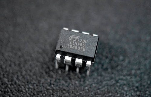
The ATtiny85 is an 8-bit RISC microcontroller that is widely popular. Because of its great functionality in such a compact size has become the primary choice for professionals and developers. It’s an 8-pin (PDIP) microcontroller with nearly all of the functionality that any microcontroller should have, including built-in FLASH, EEPROM, SRAM, SPI, IIC, ADC, etc. PWM, timer, comparator, IO, and so on. These will be discussed briefly later, but define the ATtiny85 Microcontroller first.
What is an ATtiny85 Microcontroller?
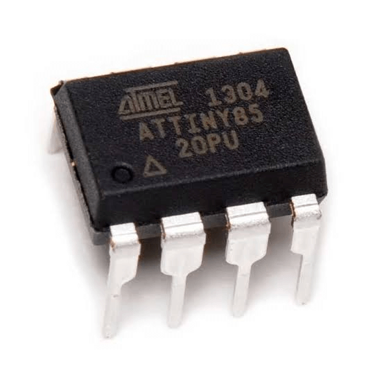
The ATtiny85 Microcontroller is a high-performance 8-pin AVR microcontroller based on the RISC advanced CPU architecture. It comes in two package kinds that can be used to interact with and control a variety of devices and sensors. It uses little power and is compact, having an 8-Kbyte program memory, an EEPROM, and 512-Kbyte RAM for storing the code of the provided instruction.
The watchdog timer is widely used in embedded and automated systems, which is the microchip’s key safety function. It’s a popular microcontroller with a lot of functionality. It’s a tiny microcontroller that can run a variety of program codes.
It’s also known as a little Arduino chip having a limited number of I/O pins, flash/program memory, SRAM, and EEPROM. Instead of using the ATmega328p or Arduino board for a simple code, the ATtiny85 microcontroller chip is used. Three analog input pins are used from these limited I/O pins to collect input from sensors.
ATtiny85 Microcontroller Specifications
ATtiny Microcontroller Specifications are as follows
- It is an advanced RISC architecture design with high performance.
- It uses an 8-bit CPU
- It has 8 number of Input-Output (I/O) pins
- It contains 8 programmable Input-Output (I/O) pins
- Its operating voltage ranges from +1.8Volts to +5.5Volts and +2.7Volts to +5.5Volts (absolute supply voltage is maximum +6Volts)
- The DC Current per I/O pin is a maximum of 40mA.
- The DC Current flow through GND and VCC pins is of a maximum of 200mA
- It operates at a temperature of -55°C to +125°C
- Communication Interfaces
- The master/slave SPI Serial Interface is used to program the ATtiny Microcontroller (5, 6, and 7 pins)
- I2C, or Two-Wire Serial Interface, links sensors, and auxiliary devices. (5 and 7 pins)
- The Universal Serial Interface is used to communicate with other controllers. (5, 6, and 7 pins)
- It is missing the UART Interface.
- There are four channels with a 10-bit ADC resolution and one Analog Comparator.
- It has two 8-bit counters that function as a timer module.
- There are four PWM outputs.
- The external oscillator has a frequency range of 0-20MHz (for ATtiny 85) and 0-10MHz (for ATtiny 86). (For ATtiny85V)
- With an internal calibrated R-C oscillator, the frequency range of the internal oscillator is 0-8MHz.
- The CPU operates at 1MBPS (1MHz)
- The flash or program memory has an 8Kbyte capacity (10000 erase/write cycles).
- Internal SRAM memory is 512 bytes incapacity.
- The EEPROM is 512 bytes in capacity and can be programmed in-system.
- A program lock and a watchdog timer are included.
- Power down, ADC noise reduction, and idle modes are among the three power-saving modes available.
- There are 32 registers in it.
- The current usage is 300 microAmps when operating at 1.8V. The current usage is 0.1 microAmps in the 1.8V power-down mode.
- It has four channels of 10-bit ADC.
Alternative ATtiny85 microcontrollers include the ATtiny45, ATtiny25, ATtiny25V, ATtiny85V, and ATtiny45V microcontrollers.
The ATtiny45 Microcontroller is a popular and inexpensive 8-pin AVR controller with RISC advanced architecture that can be programmed using the AVR IDE. It has 4 Kbytes of program memory. It can be utilized in mobile embedded systems because it offers multiple power-saving modes. It has a low-power controller that gives outstanding performance.
ATtiny85 pinout
The pinout of the ATtiny85 is described below:
Pin 1 (PB5)
It’s for analog pin ADC0, which is used with analog sensors.
Pin2 (PB3)
It’s for a crystal oscillator XTAL1 and an analog pin ADC3.
Pin3 (PB4)
It is utilized for analog pin ADC2 and crystal oscillator XTAL2.
Pin4 (GND)
It should be connected to the Ground.
Pin5 (PB0)
This pin serves as a MOSI connector (Master Out Slave In). It can be utilized as a master line for SPI communication and an SDA line for I2C communication.
Pin6 (PB1)
MISO is the function of this pin (Master In Slave Out). It can convey data to the master through a slave line.
Pin 7 (PB2)
This can be used as SCK and SCL for SPI and I2C communications.
Pin 8 (Vcc) is used as Vcc Pin & 5V is applied.
A detailed description of the pins
Power
The ATtiny85 has two pins for power. The power supply is connected to one, while the Ground is connected. The ATtiny’s power source must not exceed the rated voltage.
Pin8– Vcc
Pin4-GND
Oscillator/Clock
The internal clock of the Attiny85 is 8MHz, and its clock value ranges from 0 to 8MHz. It may, however, increase the frequency of its oscillator to 20MHz. As a result, it should be linked to the oscillator pins to increase the oscillator value.
GPIO2– XTAL1/CLKI
GPIO3-XTAL2/CLKO
Digital input/output
Any pin on the ATtiny85 can be used for input and output signals, but it must be specified in the software beforehand. These pins serve as bidirectional input/output connections. Aside from the power supply pin, every pin can be used for input/output.
GPIO5- PB0
GPIO6- PB1
GPIO7- PB2
GPIO2- PB3
GPIO3- PB4
GPIO1- PB5
Interrupt
ATtiny85 has one interrupt pin. This pin can be controlled by any sensor output or manually via a button.
GPIO7- INT0
SPI
The SPI pins on Attiny85 are:
GPIO5- MOSI
GPIO6-MISO
GPIO7- SCK
GPIO1- Debugging wire(DW)
- MOSI is used to send the data
- MISO is used for receiving the data
- SCK for the clock
- DW for programming
I2C
Attiny85 also supports the I2C communication protocol. A single line delivers and receives data via this protocol, while another line provides a clock pulse that keeps data in sync with the time. The I2C pins are:
GPIO5- SDA(Data)
GPIO7- SCL(Clock)
Timer
Timer 0 and Timer 1 are two timers on the ATtiny85 to count the clock pulses. These two clocks use the internal clock, although an external clock pulse can control the Timer 0.
Both of these timers are 8-bit. The pins for the Timers are:
GPIO7-Timer 0
Counter/Timer and PWM
The abbreviation PWM stands for Pulse Width Modulation. There are four PWM channels on the Attiny85.
Several specific pins on the Attiny85 can be utilized with the internal PWM signal input to drive external power efficiently.
The Dead Time Generator is a set of pins that function according to a specific time until it approaches zero; the timer counts and compares the value.
Timer 0 and Timer 1 are utilized in ATtiny85 to count two dead generator values, and the output signal is non-overlapping.
GPIO-OC1B
GPIO-OC1B’
GPIO-OC0B
GPIO-OC0A
GPIO-OC1A
GPIO-OC1A’
Analog Comparator
The Attiny85 features an inbuilt analog comparator that can compare analog signals in both inverted and non–inverted modes. The comparison outcome is kept in the register and can be utilized for other reasons. Attiny85 has the following analog comparator pins:
GPIO5-AIN0
GPIO6-AIN1
Analog to Digital Converter
In Attiny85, there are four analog input channels available.
The analog signal is transformed into a digital signal with a 10-bit resolution. ATtiny85 translates analog data at a pace of 65-260us, which is fast enough to update the system every second.
The analog input voltage is determined by the power supply voltage, which may result in external device problems. To eliminate this error, an analog reference pin is employed. As a result, the system receives information regarding the voltage reference’s maximum and minimum voltage levels. The reference and analog input voltage should not exceed the controller’s maximum power handling capacity. Analog pins consist of:
GPIO1-ADC0
GPIO7-ADC1
GPIO3-ADC2
GPIO2-ADC3
GPIO5-Vref
Reset
External and internal resets are available on the Attiny85. This can be done from an external pin or on a specific condition applied by the software.
ATtiny85 microcontroller Peripherals
The controller contains numerous modules, each of which operates independently on registers. You can read the datasheet for more details on their programming registers.
Brownout Reset
The controller comprises several modules, each of which operates on its registers. More information about their programming registers may be found in the datasheet.
Watchdog Timer
In most microcontrollers, it is one of the best resetters. Only instructions will be supplied to activate it at the program’s start. It will not affect the controller unless it stops working, at which point the watchdog timer will reset the ATtiny85 and restart it.
Debug Wire
Although we discussed SPI programming for the PIC in SPI pins, a debug pin will be utilized to program any controller using the SPI protocol. This pin will cut the program instructions from the CPU and then program the non-volatile memory. The use of a debug pin will be limited to the presence of SPI pins on the controller; otherwise, it will be useless.
Deadtime Generator
The ATtiny85’s output pairs of PWM allow the controller to manage the external control switches safely. It uses a PWM pulse and a zero check with the Dead Time Generator to ensure the counter is complete. The Dead Timer Generator aids in non-overlapping output.
Self Programing.
The ATtiny85 has a self-programming option for setting the controller’s bootloader. If a commercial product’s memory fails, this self-programming method comes in handy. It can also be utilized during the bootloader to get specialized data. The controller must first enable the self-programming capability before using it; else, the feature will not work.
Conclusion
The ATtiny85 is utilized in various embedded applications, and when programmed with the Arduino IDE, it can do a variety of tasks. It has fewer pins, is less expensive, and consumes less power overall.
Overall, the ATtiny85 is a cost-effective and efficient microcontroller that fits your technological requirements.
For more details on ATtiny85 microcontroller, contact us at ICRFQ, we manufacture the best electrical components in China.
If you want to find more Electronic Components Distributors, please check out the following articles:
Electronic Components Distributors In the USA
Electronic Components Distributors In UK
Electronic Components Distributors In China
Electronic Components Distributors In India
Electronic Components Distributors In Singapore
Electronic Components Distributors In Malaysia
Electronic Components Distributors In Vietnam
Electronic Components Distributors In South Korea
- Where to buy IC chips? The Best Guide? - March 26, 2024
- Breaking Down Barriers: Overcoming Obstacles in Cross-Border Electronic Component Trade - March 4, 2024
- Everything You Need to Know About Amplifier IC Chips - March 4, 2024


