
Last Updated on October 22, 2023 by Kevin Chen
BGA stands for “ball grid array”. It is a type of integrated circuit packaging in which ball-shaped chips are soldered on a board. Ball grid array is the most common type of IC packaging and is used for various electronic applications.
While BGA may seem like a simple packaging option, it has some unique challenges and drawbacks. This article covers everything you need to know about BGA packages, including common BGA variants, why BGA is used, what BGA chips can be used for, its pros and cons, types, manufacturing process, and more. Let’s get started.
What does a BGA chip do?
A BGA chip is used for various electronic applications. It is used in computers, mobile phones, digital cameras, and other electronic products. They are commonly used in the latest CPU microprocessor packages.
BGA chips are usually made from a multilayer printed circuit board (PCB) with solder balls attached to the board to represent each connection of the integrated circuit.
These solder balls are the electrical contacts of a BGA package and form a grid on the surface of the PCB.
BGA packaging is used for high-density interconnects and allows for increased performance of electronic devices.
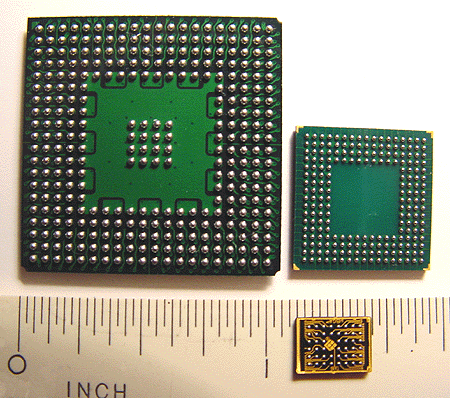
What does a typical BGA chip look like?
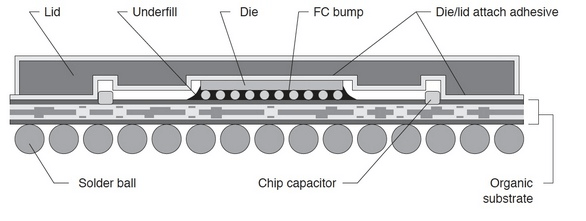
The BGA package is a rectangular-shaped chip. It has a single die on it and the die is usually mounted in the middle of the package. The ball grid array (BGA) package consists of two interconnected parts, namely the core and substrate.
The core is a sheet of metal or ceramic which acts as a support for the active device(s). The substrate is generally made from glass or plastic and consists of preformed solder balls.
It comes in two variants, namely unidirectional and bidirectional. In a unidirectional BGA, there are no solder balls in both the directions of PCB tracks, but only one direction has solder balls. In a bidirectional BGA, there are solder balls in both the directions of PCB tracks.
Components of a BGA chip
The main components of a BGA chip include;
Die
The die is the actual semiconductor device that is used to perform the function of the chip. It consists of transistors, resistors, diodes, capacitors, and other electronic components.
Die is usually made from silicon. The die is covered by a protective layer called ‘silicon dioxide’ or ‘oxide’. It prevents contamination from other substances. The die is then attached to the package substrate using a technique called wire bonding.
Ball Grid Array (BGA) Package
The BGA is the container that holds all the components of the chip. It consists of a substrate with solder balls present on its surface. The solder balls are the electrical contacts of a BGA package and form a grid on the surface of the PCB.
The number and density of solder balls depend on the size of the BGA package. For example, if we have a 0.5 mm pitch BGA then there would be 15000 solder balls present in it, whereas if we have a 1 mm pitch then there would be 3000 solder balls in it.
The main purpose of using a BGA package is to increase performance while using less space. Hence, they are mostly used in high-density interconnects like CPU microprocessor packages and memory chips.
Solder balls
Solder balls are small spherical balls of solder which are present on the surface of the substrate. They are present in a grid pattern, hence the name. These solder balls are used to connect the components to the PCB.
In a BGA package, there is a core substrate and each solder ball is attached to it using an adhesive called ‘liquid epoxy’. The liquid epoxy is cured by heating it up to a specific temperature, which depends on its composition.
The curing process takes some time and hence during this time, the BGA package cannot be used for any purpose. The curing time also depends on the size of the BGA package and its composition.
The number of solder balls present in a BGA package depends on its size and pitch, as mentioned above.
Substrate
A substrate is a board on which the BGA package is attached. It is a thin piece of glass or plastic. It has a base layer that contains the solder balls, and a top layer that holds the substrate in place. The top layer of the substrate can be made up of any material like copper, aluminum, nickel, titanium, etc., depending on the requirement of the customer.
Pitch
Pitch refers to how many solder balls are present in a square inch. In other words, it is how many solder balls are present in one square inch of space on the PCB. The pitch varies across different BGA packages and they are specified by their manufacturers as per their requirements.
Trace
Trace is the part of the BGA chip package which connects the device to the motherboard. It is made up of copper wires, which are used to carry signals from one component to other components on the PCB.
The trace width is also specified by its manufacturers and it varies across different BGA packages.
BGA chip families/types
Before you buy BGA chips, you should know that they are not all the same. They are classified into different variants and packages based on their physical and electrical properties.
The three major BGA types are;
PBGA
PBGA stands for plastic ball grid array. As the name suggests, it uses plastic as the main packaging material. The package is divided into two halves, each half having a number of balls to hold the chips inside. The ball size is 0402 and 0201, which are the most common sizes used in BGA packages.
Advantages
The main advantages of PBGA include;
-Low cost since the materials used for the chips are easily available
-Excellent thermal compatibility
-Delivers excellent electrical performance
Disadvantages
PBGA chips tend to be sensitive to humidity.
CBGA
The acronym CBGA stands for Ceramic ball grid array. The main materials used in this packaging are ceramic balls.
Advantages
The main advantages of CBGA include;
-Excellent electrical performance, thermal and physical characteristics over PBGA
-Higher reliability than PBGA chips
-High-density packaging, which may reduce system cost and size
Disadvantages
The main disadvantage of CBGA is that the ceramic balls tend to break easily. This may cause a short circuit on the PCB, which could lead to damage to other components on the board. Hence, it should be packaged carefully.
TBGA
TBGA stands for Thermally enhanced ball grid array. The main materials used in this packaging are thermally grown SiO and Si.
Advantages
The main advantages of TBGA include;
-Excellent thermal properties or heat dissipation over PBGA
-Good electrical performance and reliability
-High-density packaging, which may reduce system cost and size.
Disadvantages
The main disadvantage of TBGA is that the thermal growth may cause the SiO and Si to crack, which could lead to short circuits on the PCB, which could lead to damage to other components on the board. Hence, it should be packaged carefully.
BGA chip inspection
Before being shipped to the target clients, BGA chips must be inspected. This is done to ascertain the features and parameters of the chip. X-ray inspection is the most ideal method for inspecting the chips.
The key parameters that are revealed during the BGA chip inspections include;
-Solder joint radius: This refers to the distance between the solder joints on the chip.
-Chip height: This refers to the distance of the chip from the PCB.
-Chip width: This refers to the distance of the chip from its nearest solder joint.
-Solder joint density: Density is defined as a measure of how close together two objects are in relation to each other. In this case, it is a measure of how many solder joints there are per unit area.
-Solder joint pitch: This is defined as a measure of how far apart two solder points are on a given board. It is defined as (board pitch*number of chips).
-BGA pad density: This is defined as (the number of BGA pads/unit area) and represents how many BGA pads per unit area there are on your board. Note that this parameter only applies to boards where BGA pads are used for I/O connections or where BGA pads are used for interconnecting other boards with.
-Deviation from the circular form: This is defined as (bend radius+pitch+width) and represents the deviation from the ideal circular shape of BGA chips.
-BGA rut count: This is defined as the number of BGA ruts on a given board.
-BGA rut pitch: This is defined as the distance between two BGA ruts on a given board.
How do I align my BGA chip?
BGA chip alignment refers to the process of aligning BGA chips on a board so that all BGA chip edges are aligned with the edges of the board. The reason that this is important is that it allows proper electrical connection between the BGA chip and the board.
There are several methods used to align BGA chips on a board. The most common method consists of using a machining fixture to hold all the BGA chips in place.
Another method uses a special fixture that holds all of the BGA chips in place, but also allows them to be rotated and moved along their X-Y axes as well as rotated around their Y-Z axes. A third approach involves using a CNC machine with a rotary table that can move all of the components along the X, Y, and Z axes individually.
The alignment process for each method starts by placing all of the components on the work surface and moving each component from one position to another in an attempt to get them lined up perfectly straight (or at least close enough). Once they are lined up, the BGA chip is aligned using the method that is used to align it during the manufacturing process.
Does the BGA chip need solder paste?
Yes, BGA chips do need solder paste. BGA solder paste is a special type of solder that has a smaller diameter and a different melting temperature than normal solder.
The BGA chip has pads that are either not connected or connected to other pads on the board. The BGA chip will require soldering in order to complete the circuit.
The solder paste holds the components in place while the heat from the iron melts it, allowing the components to stay in place until they are soldered.
BGA chip Component mounting
Component mounting refers to the process of placing the BGA components on the board.
The components are placed using a PCB mounting tool. The board mounting tool is a special type of wire-bonding tool that can be used to place BGA components on the PCB.
The BGA component has pads that are either not connected or connected to other pads on the board. The BGA component will require soldering in order to complete the circuit.
When placing components, it is important to ensure that they are placed in their right location and oriented properly.
If a component is not oriented properly, it will have poor performance or even cause damage to the circuit due to short circuits.
BGA chip Connector types
There are two types of connectors used for BGA components: male and female connectors. Both types of connectors can be used for both through-hole and surface mount connections, depending on how they are attached to the PCB.
BGA chips use both male and female connectors.
The male BGA connector is designed to mate with a female BGA connector. If a male BGA component is connected to a PCB using a female BGA connector, it will have poor performance or even cause damage to the circuit due to short circuits.
To ensure that the male and female connectors are properly oriented, it helps if both connectors are placed on top of the PCB before soldering them in place.
Where to buy BGA chips?
The BGA is a very common type of semiconductor device, but it is not very popular. This means that there are relatively few suppliers of BGA chips.
Even if you have the correct components, it is difficult to find a supplier that can provide the right BGA chip for your application.
This means you will need to perform some research and contact many suppliers before finding the right one.
A smoother route to take is choosing a BGA chips sourcing agent. They will do all the sourcing for you. For instance, if you choose a BGA sourcing agent in China, such as ICRFQ, we will find the right manufacturer and supplier for you.
If you want to find more Electronic Components Distributors, please check out the following articles:
Electronic Components Distributors In the USA
Electronic Components Distributors In UK
Electronic Components Distributors In China
Electronic Components Distributors In India
Electronic Components Distributors In Singapore
Electronic Components Distributors In Malaysia
Electronic Components Distributors In Vietnam
Electronic Components Distributors In South Korea
- Where to buy IC chips? The Best Guide? - March 26, 2024
- Breaking Down Barriers: Overcoming Obstacles in Cross-Border Electronic Component Trade - March 4, 2024
- Everything You Need to Know About Amplifier IC Chips - March 4, 2024


