
Last Updated on October 22, 2023 by Kevin Chen
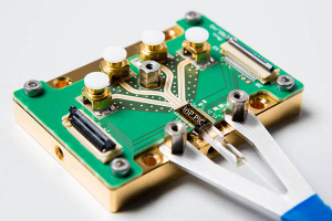
Image Source: Gijs van Ouwerkerk
A photonic integrated circuit (PIC) is a chip with photonic components that work with light instead of electrical components that create a functional circuit and are found inside your smartphone, computer, and other electronic devices.
In an electronic chip, the flux of electrons travels through electrical elements like transistors, resistors, inductors, and capacitors; in a photonic chip, the flux of photons travels through optical elements like waveguides, which are analogous to resistors or electrical wires, lasers, polarizers, and phase shifters.
What Is Integrated Photonics?
Utilizing light for tasks that electronics have historically handled is known as integrated photonics (IP). It can be employed in various industries, including telecommunications (5G networks), biosensors to expedite medical diagnoses, and the automotive industry (LiDAR). IP is the integration of numerous photonic functionalities onto a Photonic Integrated Circuit (PIC) over silicon, indium phosphide (InP) or silica substrates utilizing automated wafer-scale generic integration technology. These optical functions are significantly more efficient and reliable thanks to integrated photonics, which also decreases weight, size, and power usage.
Electronics versus Photonics
Understanding the similarities and differences between IP and conventional electronic circuits will help you better grasp this technology. Photonics uses photons to control them in the same way that electronics control electrons on a chip. The fundamental building blocks of light are photons.
By allowing electrons to move freely through the circuit, conventional integrated circuits (ICs) conduct electricity. Subatomic particles called electrons have a negative charge and can interact with other particles and electrons. As electrons pass through circuits, these interactions slow them down, limiting the amount of information that can be communicated. They also produce heat, which results in energy and information losses.
Photons are used in photonic integrated circuits (PICs). Almost no other photons interfere as photons move at the speed of light. PICs are substantially more energy-efficient than their IC counterparts thanks to this significant increase in bandwidth (the rate at which data is transferred) and speed of the circuit without significant energy losses.
Like metallic wires, confine and direct electrical signals, integrated photonic components use “waveguides,” which direct light (via total internal reflection) in the required directions. A PIC offers functionality for information signals on optical wavelengths, often in the visible spectrum or near-infrared between 850 and 1650 nm.
Waveguides connect the components of a PIC. The chip components can be active or passive, such as couplers, switches, modulators, and multiplexers. The small and reliable photonic device integrates and fabricates these components onto a single substrate.
The fundamental fabrication tool utilized in PICs and electronic circuits differs significantly. The transistor is the primary component of an integrated circuit used in electronics. However, there isn’t a single main device in PIC that predominates in fabrication. The PIC will have a variety of fabrication devices depending on its intended use.
What issue is resolved by a photonic integrated circuit, and how does it operate?
PICs use a laser source to inject light that drives the components, much like turning a switch to inject energy that powers electrical components. Integrated photonic technology, commonly referred to as “more than Moore,” is a technique that uses light rather than electricity to get around some of the drawbacks of electronics such integration and heat generation. With the use of this technology, gadgets can now transmit data at higher and quicker speeds. PICs feature advantages including shrinkage, faster speed, less heat effects, huge capacity for integration, and compatibility with current processing flows that enable high yield, mass production, and lower prices. Among the many applications of integrated photonics are data transmission, sensing, the auto industry, and astronomy.
Applications
PICs use a laser source to inject light that drives the components, much like turning a switch to inject energy that powers electrical components. Integrated photonic technology, commonly referred to as “more than Moore,” is a technique that uses light rather than electricity to get around some of the drawbacks of electronics such integration and heat generation.
This technology advances devices to the next level, enabling faster and larger data transmission rates. PICs feature advantages such as downsizing, accelerated speed reduced heat effects, and compatibility with current processing processes that enable high yield, , enormous capacity for integration, mass production, and lower prices. The topic of integrated photonics has many uses, including data transmission, sensing, the automobile sector, and astronomy.
Healthcare And Medicine
Integrated photonics opens the door to lab-on-a-chip (LOC) technology, reducing wait times and putting diagnosis in the hands of physicians and patients by using advanced biosensors and more reasonably priced biomedical diagnostic tools. The diagnostics platform from SurfiX Diagnostics offers numerous point-of-care assays based on an ultrasensitive photonic biosensor.
Similarly, Amazec Photonics has created a fiber optic sensing technique using photonic chips that allows for high-resolution temperature detection (fractions of 0.1 milliKelvin) without injecting the temperature sensor within the body. Medical professionals can measure cardiac output and the volume of blood in circulation outside the body in this way. The ‘OptiGrip’ device from EFI is another example of optical sensor technology because it gives surgeons more control over tissue feel during minimally invasive procedures.
Automotive And Engineering Applications
PICs can be used in sensor systems, such as Lidar (light detection and ranging), to monitor the area around moving vehicles. In-car connectivity can also be provided using Li-Fi, a technology that works similarly to WiFi but uses light. This technology makes it easier for vehicles and urban infrastructure to communicate to increase driver safety. For instance, contemporary automobiles can pick up traffic signs and alert drivers to the posted speed limit.
Engineers can employ fiber optic sensors to measure various parameters, including pressure, temperature, accelerations, vibrations, and mechanical strain. Sensors from PhotonFirst use integrated photonics to measure the temperature of electric vehicle batteries, the pressure on infrastructure, and changes in an airplane’s shape.
Agriculture And Food
To cut waste and detect diseases, sensors are used in agriculture and food sector advancements. The food supply chain can now identify disease, maturity, and nutritional content in fruit and plants thanks to light sensor technology powered by PICs. In addition to measuring CO2 emissions, it can assist food producers in determining soil quality and plant growth. A new miniature near-infrared sensor created by MantiSpectra can examine the chemical composition of items like milk and plastics. It is so small that it can be placed inside a smartphone.
Fabrication And Materials
PICs are currently produced on the compound and standard element semiconductors to nonlinear crystal and dielectric materials. The specific application requirements determine the most appropriate substrate material because each material has unique advantages and disadvantages. For instance, flexible chalcogenide glass with integrated flexible lithium niobate can create photonic crystals with mechanical flexibility.
The materials’ transparency, refractive index, and direct light generation capabilities determine the completed PIC’s characteristics and applications. The bend loss and bend radius of the material also influences the PIC properties. The bend radius specifies how much fiber may bend before it breaks. In contrast, bend loss represents propagation losses (decrease in power density) in an optical fiber (or another waveguide) due to bending. Indium phosphide (InP)-based monolithic integration and silicon photonics are currently the two most widely used substrates, though silica (SiO2) and silicon nitride (SiN) are also becoming more popular.
Indium Phosphide (InP)
The most well-established PIC platform is indium phosphide (InP). Interferometers, high-performance amplifiers, lasers, modulators, and detectors assembled with interferometers on a single chip allow for the integration of active and passive elements in the 1.1 – 1.6 m spectral window. Data transmission, precise metrology (like LIDAR in autonomous vehicles), spectrometry, and imaging are all used inP integrated photonics.
Many of the most influential studies on InP have been conducted in the Netherlands, and several institutions and research teams are still at the forefront of the field. Leading manufacturers of Indium Phosphide-based photonic components include the Eindhoven-based Smart Photonics foundry. InP PICs are being tested and used more widely by businesses and researchers thanks to the foundry and the services it provides.
Silicon Photonics (SiPh)
Silicon photonics (SiPh) is an essential component in developing integrated photonics, building on the success of silicon (Si) as the basis of IC reliability. Since most integrated circuits already use silicon as their substrate, silicon photonic devices can be created using existing available semiconductor fabrication techniques. This enables the chip to integrate optical and electronic components to produce hybrid devices.
Si is ideal for fiber optic telecommunication systems with a 1.55-micrometer wavelength because it is transparent to infrared light with wavelengths above about 1.1 micrometers (m). Additionally, it has a refractive index that is substantially higher than silicon oxide’s (1.5), at roughly 3.5, allowing for much light confinement in silicon structures implanted in silicon oxide (waveguides). Si is a good candidate for use in telecom because of these qualities.
Silicon Nitride (SiN)
Systems based on silicon nitride (SiN) have lately gained popularity because to their wide transparency window (from visible to MIR) and relatively low optical losses as compared to other PIC platforms. As a result of its extremely low light intensity loss in the waveguide, tiny bend radii, and tunable polarization, silicon nitride (SiN) excels at passive light processing in the visible, near-infrared (NIR), and IR ranges. Through PIC-level hybrid integration techniques, active components manufactured on a different technological platform (such as InP) can be connected to SiN PICs into the same package if the application needs it.
The lowest propagation losses observed for silicon nitride waveguides are found in the unique TriPleX waveguide design from the Dutch company Lionix International (0.1 dB/cm down to 0.1 dB/m). It works across a wide spectrum of wavelengths, from 405 nm to 2350 nm. They also created a proprietary tapering technique that transforms low contrast modes for the best fiber coupling into high contrast modes for tiny bending radii.
Large-scale research initiatives are being conducted to reduce the number of assembly stages now required, offer lossless material transitions, and develop more affordable manufacturing processes.
Lithium niobate (LiNbO3)
A nonlinear crystal material called lithium niobate (LiNbO3) is ideal for devices executing nonlinear operations or operations that benefit from this material feature. Acousto-optic transducers or electro-optical modulators are two examples. On lithium niobate substrates under lithographic control, waveguides can be created. Amplifiers and lasers can be created by “doping” lithium niobate with rare-earth ions.
Birefringence is a feature of LiNbO3, which means that the polarization direction affects the material’s refractive index. As a result, polarization control is made possible, which may be applied to filtering or other comparable tasks. This characteristic makes constructing polarization-independent devices, frequently necessary for optical fiber communications, more challenging.
Conclusion
A developing area of technology called integrated photonics has already shown tremendous future potential in numerous fields. The leadership of PhotonDelta is supporting and promoting a large portion of the developments/scale-ups and pertinent R&D in this burgeoning business in the Netherlands. PICs’ efficiency and speed will keep rising, generating disruptive innovation—enabling (radically) new products and markers—as well as enhancing current systems.
For further information or to place an order for a photonic integrated circuit (PIC), contact us at ICRFQ. We’ll make sure you pay a reasonable price for the product.
If you want to find more Electronic Components Distributors, please check out the following articles:
Electronic Components Distributors In the USA
Electronic Components Distributors In UK
Electronic Components Distributors In China
Electronic Components Distributors In India
Electronic Components Distributors In Singapore
Electronic Components Distributors In Malaysia
Electronic Components Distributors In Vietnam
Electronic Components Distributors In South Korea
- Where to buy IC chips? The Best Guide? - March 26, 2024
- Breaking Down Barriers: Overcoming Obstacles in Cross-Border Electronic Component Trade - March 4, 2024
- Everything You Need to Know About Amplifier IC Chips - March 4, 2024


