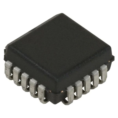
EPC2LI20
Part Number: EPC2LI20
Manufacturer: Intel / Altera
Description: FPGA – Configuration Memory IC – Ser. Config Mem Flash 1.6Mb 10 MHz
Shipped from: Shenzhen/HK Warehouse
Stock Available: Check with us
ICRFQ.com - Electronic Components Distributor in China Since 2003

Part Number: EPC2LI20
Manufacturer: Intel / Altera
Description: FPGA – Configuration Memory IC – Ser. Config Mem Flash 1.6Mb 10 MHz
Shipped from: Shenzhen/HK Warehouse
Stock Available: Check with us
| Datasheet | |
|---|---|
| Category | Integrated Circuits (ICs) |
| Family | Memory – Configuration Proms for FPGAs |
| Manufacturer | Altera |
| Series | EPC |
| Packaging | Tube |
| Part Status | Active |
| Programmable Type | In System Programmable |
| Memory Size | 1.6Mb |
| Voltage – Supply | 3 V ~ 3.6 V, 4.5 V ~ 5.5 V |
| Operating Temperature | -40°C ~ 85°C |
| Package / Case | 20-LCC (J-Lead) |
| Supplier Device Package | 20-PLCC (9×9) |
The in-system-programmable, high-density, high-performance EPLDs that make up the MAX 9000 family’s EPC2LI20 are referred to as the MAX 9000 family EPC2LI20. These EPLDs are based on the third iteration of the MAX architecture that Altera has developed. The MAX 9000 family, based on EEPROM and manufactured using advanced CMOS technology, offers anywhere from 6,000 to 12,000 useable gates, pin-to-pin delays as short as 10 nanoseconds, and counter rates that can reach up to 144 MHz.
Programmable logic devices (PLDs) with high performance are based on CMOS EEPROM and constructed on third-generation Multiple Array Matrix (MAX) architectures.
An electronic component known as a programmable logic device, or PLD, is utilized to construct digital circuits that may be reconfigured. A PLD, on the other hand, has an undetermined function at the time it is manufactured, in contrast to digital logic, which is built using discrete logic gates that have predetermined functionalities. It is necessary first to program the PLD to carry out the intended function before it can be employed in a circuit.
This apparatus comprises programmable AND gate arrays and OR gate arrays, both of which need to be programmed by the user to get the desired output.
PALs use an OR gate array with a predetermined logic set, but an AND gate array can be programmed according to the user’s specifications. As a result, The sum-of-products notation expresses the output as a combination of the inputs.
These devices had qualities comparable to those of PALs, in addition to being able to be electrically erased and reprogrammed. This essential characteristic proved advantageous, as it made the prototype design noticeably simpler, which, in turn, cut down the time needed to bring the product to market.
CPLDs include more programmable logical elements and are denser than PALs. Through the utilization of the interconnecting network, it will be the user’s responsibility to set up the connections required between the macro cells. In this particular scenario, logical components that a sum-of-product has determined are combined to build structures that reduce the total number of input-output (IO) pins.
This makes it possible to construct logic designs with a higher degree of complexity despite having a slower propagation speed when compared to PALs. This is made possible by the fact that the propagation speed is slower. Since these have stable timing characteristics, they are ideally suited for use in control applications that are high-performance and mission-critical. When it comes to implementing combinational logic-based systems, CPLDs are highly recommended.
Field programmable gate arrays, also known as FPGAs, utilize gate array technology instead of PROM technology in early PLDs. An interconnection matrix traverses the entirety of the device, allowing customizable logic blocks (CLBs), which are the building blocks of these devices, to communicate with one another. FPGAs can carry out their operations thanks to the look-up tables (LUTs) and flip-flops within the CLB.
The CLBs will have been configured to carry out the user’s intended logical function once the user has utilized the interconnection matrix to connect one or more logic blocks. In addition, they come equipped with input-output (I/O) ports, which make it much simpler to program and debug the whole architecture. These input and output ports are incorporated into the design.
In addition to developing designs based on combinational logic, these devices can also build sequential designs based on state machines. These gadgets allow for the creation of any of these two sorts of designs. FPGAs can realize more complex designs than those that can be realized using CPLDs.
This is because FPGAs have a higher density than CPLDs. In addition, field-programmable gate arrays, or FPGAs, provide the customer with the flexibility to build or re-design the logic even after the device has been deployed in the working field, which is how they got their name. This feature allows the customer to change the logic even after it has been implemented. On the other hand, when contrasted with CPLDs, FPGAs are characterized by much greater propagation delays.
These programmable logic devices (PLDs) can be programmed using device programs specific to each PLD. These device programs are the ones that are in charge of transferring the Boolean logic pattern onto the programmable device.
Thanks for reading. If you like this article, please explore the rest of our website for more great content like this one and learn more. If you have any questions about this article, please leave them in the comment section below, and we will do our best to respond to them.
If you need information or want to order EPC2LI20, contact us here at ICRFQ, your leading electronic components in china, and we will ensure you get the best product at the best price.
WhatsApp us