FDN306P
Part Number: FDN306P
Manufacturer: onsemi / Fairchild
Description: MOSFET P-Ch PowerTrench Specified 1.8V
Shipped from: Shenzhen/HK Warehouse
Stock Available: Check with us
ICRFQ.com - Electronic Components Distributor in China Since 2003

We make your sourcing easier!
Get A Fast Quote Worldwide!

Part Number: FDN306P
Manufacturer: onsemi / Fairchild
Description: MOSFET P-Ch PowerTrench Specified 1.8V
Shipped from: Shenzhen/HK Warehouse
Stock Available: Check with us
| Datasheet | |
|---|---|
| Category | Discrete Semiconductor Products |
| Family | Transistors – FETs, MOSFETs – Single |
| Manufacturer | Fairchild Semiconductor |
| Series | PowerTrench? |
| Packaging | Tape & Reel (TR) |
| FET Type | MOSFET P-Channel, Metal Oxide |
| FET Feature | Logic Level Gate, 1.8V Drive |
| Drain to Source Voltage (Vdss) | 12V |
| Current – Continuous Drain (Id) @ 25°C | 2.6A (Ta) |
| Rds On (Max) @ Id, Vgs | 40 mOhm @ 2.6A, 4.5V |
| Vgs(th) (Max) @ Id | 1.5V @ 250μA |
| Gate Charge (Qg) @ Vgs | 17nC @ 4.5V |
| Input Capacitance (Ciss) @ Vds | 1138pF @ 6V |
| Power – Max | 460mW |
| Operating Temperature | -55°C ~ 150°C (TJ) |
| Mounting Type | Surface Mount |
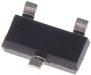
| Package / Case | TO-236-3, SC-59, SOT-23-3 |
| Supplier Device Package | SuperSOT-3 |
The P-channel 1.8V MOSFET is fabricated using the cutting-edge PowerTrench® low-voltage manufacturing method. It has been optimized for applications involving battery power management. But what is a power MOSFET exactly? Perhaps some of us have questioned the same thing, which is why we’re here: to assist. Before moving on to FDN306P, let’s review the basics of a power MOSFET. Shall we?
Metal-oxide-semiconductor field-effect transistors (MOSFETs) are often used in electronic devices, and a power MOSFET is a subset of MOSFETs that is optimized for handling high power. Good efficiency and High switching speed at low voltages are its key advantages compared to other power semiconductor devices like an insulated-gate bipolar transistor (IGBT) or thyristor. It’s straightforward to drive because it uses the same isolated gate as the IGBT. Sometimes the gate voltage has to be higher than the voltage regulated because of the low gain.
The development of MOSFET and CMOS technology, utilized in the fabrication of integrated circuits since the 1960s, allowed for the design of power MOSFETs. The power MOSFET is functionally equivalent to its lower-power sibling, the lateral MOSFET. The power MOSFET, now ubiquitous in power electronics, was developed from the original MOSFET in the 1970s.
Because of its many desirable properties, including quick switching speed, low gate drive power, easy advanced paralleling capabilities, easy application, ruggedness, easy drive, simple biasing, wide bandwidth, and simple maintenance, the power MOSFET has become the most widely used power semiconductor device in the world. In particular, it is the most popular switch for applications requiring less than 200 V. Many electronic devices rely on it, including power supply, DC-to-DC converters, and low-voltage motor controllers.
Mohamed Atalla and Dawon Kahng of Bell Labs came up with the MOSFET in 1959. The field of power electronics could finally go forward. Power designers could reach new heights of efficiency and density with successive generations of metal-oxide-semiconductor field-effect transistors.
Hitachi unveiled the original vertical power MOSFET, or VMOS, in 1969. (V-groove MOSFET). In the same year, Toshihiro Sekigawa and Y. Tarui, Y. Hayashi from the Electrotechnical Laboratory reported the development of the DMOS (double-diffused metal-oxide-semiconductor field-effect transistor) with a self-aligned gate (ETL). The audio power MOSFET was designed by Jun-ichi Nishizawa of Tohoku University in 1974; Yamaha Corporation began producing it shortly after that for use in their hi-fi amplifiers. In 1974, companies, including JVC, Pioneer Corporation, Sony, and Toshiba, began producing amplifiers with power MOSFETs. It wasn’t until 1975 that Siliconix introduced a commercially available VMOS.
The VDMOS is the offspring of the VMOS and DMOS (vertical DMOS). In 1977, John Moll and his team at HP Labs showed the benefits of the DMOS over the VMOS, including reduced on-resistance and higher breakdown voltage, by fabricating prototypes. The same year saw the debut of another DMOS variant from Hitachi, the LDMOS (lateral DMOS). From 1977 to 1983, when Hitachi was the only LDMOS producer, it was utilized in audio power amplifiers by companies like HH Electronics (V-series) and Ashly Audio for applications including playing music and broadcasting announcements. LDMOS quickly surpassed all other RF power amplifiers in use by mobile networks, including 2G, 3G, and 4G, after the debut of the 2G digital mobile network in 1995.
In 1977, Tom Herman and Alex Lidow created the HexFET at Stanford University, a Power MOSFET with a hexagonal shape. In 1978, International Rectifier began mass-producing the HexFET. Combining features of the power MOSFET and the bipolar junction transistor (BJT), Jayant Baliga of General Electric created the insulated-gate bipolar transistor (IGBT) between 1977 and 1979.
The power MOSFET, a super junction MOSFET, uses P+ columns through the N- epitaxial layer. Shozo Shirota and Shigeo Kaneda from Osaka University proposed stacking P and N layers in 1978. In 1984, David J. Coe of Philips filed for and was granted a US patent on the super junction MOSFET, which consists of alternating p-type and n-type layers.
Before the introduction of the first commercial power MOSFETs in the 1970s, various architectures had been investigated. If you look at a cross-section of a VDMOS (see Figure 1), you can see that the source electrode is positioned above the drain, producing a predominantly vertical current in the state of the transistor. The “diffusion” in VDMOS refers to the production method used to create the device; in this case, it is a diffusion process (more accurately, two diffusion processes are utilized to generate the P and N+ regions; hence the name double diffused) that yields the P wells
In contrast to the lateral MOSFET, the construction of power MOSFETs is vertical rather than planar, as is typical of most power devices. Because breakdown voltage and current ratings depend on channel dimensions, using a planar arrangement wastes silicon “real estate.” The transistor’s maximum current rating depends on the channel width.
In contrast, the voltage rating is a function of the doping and thickness of the N epitaxial layer in a vertical arrangement. This permits the transistor’s small silicon footprint to support a high blocking voltage and a sizable current.
The lateral structure of LDMOS power MOSFETs sets them apart from conventional MOSFETs. They find widespread application in RF power amplifiers for 2G, 3G, and 4G wireless cellular networks and high-end audio power amplifiers. Compared to vertical MOSFETs, they perform better in the saturated region (which is analogous to the linear part of a bipolar junction transistor). Since vertical MOSFETs are solely employed in either the On or Off states, they are best suited for switching applications.
This MOSFET with a P-Channel specification and 1.8V supply voltage leverages Fairchild’s innovative low voltage Power Trench technology. It has been improved for use in applications dealing with battery power management.
We hope you found the given information on FDN306P useful for your projects. Please explore our website for additional quality content. If you have questions regarding this or any other topic on our website, please post them in the section below, and we will respond.
Please contact ICRFQ if you have any questions or would like to place an order for FDN306P or related electronic components. Our company is China’s leading distributor of electronic components.
WhatsApp us