
Last Updated on May 1, 2022 by Kevin Chen
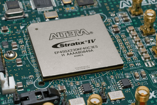
Field-programmable gate arrays (FPGAs) are gaining popularity, especially in embedded system development and deep neural networks for artificial intelligence applications. The first market-worthy field-programmable gate array having both programmable gates and programmable interconnects between gates was designed by Xilinx co-founders in 1985. PROMs and programmable logic devices (PLDs) were the forerunners to FPGAs (PLDs).
What is FPGA Chip?
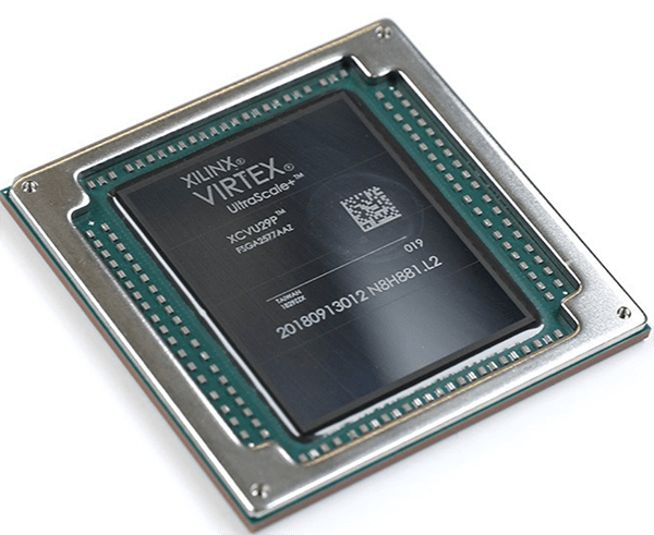
FPGA chip stands for Field Programmable Gate Array, an Integrated Circuit that may be customized to perform multiple jobs as needed. An FPGA, for example, can be designed to act as a CPU and then modified to function as a GPU, hardware video encoder, or something else. The argument is that an FPGA can theoretically be designed to perform the same tasks as any other Digital Integrated Circuit.
Consider the analogy of today’s microcontrollers. They can be programmed multiple times with various software (firmware), and their functioning varies depending on the firmware used. FPGAs are comparable to programmable logic devices (PLDs), except they can be repeatedly programmed with different hardware designs (hardware descriptions). Their functionality changes as the hardware design run on them. Of course, if you program with a design describing a microcontroller, FPGAs can serve as microcontrollers.
Field Programmable Gate Array (FPGA) is an acronym for Field Programmable Gate Array. FPGAs are field programmable, which means they may be programmed outside of the IC fabrication plant, at home, at the office, or anywhere else. FPGAs contain many logic gates and flip-flops that users can connect according to design requirements, causing the FPGAs to function as intended. The gates and flip-flops are organized into Configurable Logic Blocks (CLBs) regarding the technical side of things. On FPGAs, there are hundreds of CLBs packed in a sea of programmable connection matrices. Using this programmable interconnect matrix, the CLBs are connected to create a specific circuit capability.
How Does an FPGA Chip Work?
Internal hardware pieces with user-programmable interconnect to make up an FPGA chip, which allows it to be customized for a given purpose. These interconnects can be reprogrammed, allowing the FPGA to adapt to design modifications or enable a new application over the part’s lifetime. The FPGA is programmed during manufacturing, but it can be reprogrammed afterward to reflect device modifications.
An FPGA comprises a matrix of customizable logic blocks (CLBs) linked together by programmable interconnects. Two 16-bit function generators, one 8-bit function generator, two registers (flip-flops or latches), and reprogrammable routing controllers make up the primary FPGA cell (multiplexers). CLBs are used to implement macros and other functions that have been designed.
Because FPGAs, unlike processors, can perform several operations simultaneously, distinct processing operations do not compete for the same resources. Each independent task is given to its area of the chip and can operate independently of the other logic blocks. As a result, as more activities are introduced, the performance of one application area remains unchanged.
The internal configuration of the FPGA is set by software, or “firmware,” as it is sometimes referred to. FPGAs can be reprogrammed in the field as application or functionality needs to change.
Hardware Description Languages like Verilog HDL and VHDL are used to program FPGAs. FPGAs differ from ASIC ICs in that they can be reprogrammed, whereas ASIC ICs are built to perform specific jobs.
Early in the design phase, deciding whether an FPGA-based design should be adopted is necessary. This should be considered if the chip needs to be reprogrammed later in the design process or even after manufacture. Manufacturers may choose an FPGA-based design early in the development cycle to find flaws, then transition to an ASIC once the design is stable.
What language do you use to program FPGA?
Hardware Description Languages (HDL) like Verilog, VHDL, and System Verilog are commonly used to code FPGA designs. These are the most popular languages. However, there are much more advanced than those listed above, such as SystemC, Migen, MyHDL, Chisel, SpinalHDL, MATLAB, etc. High-Level Synthesis (HLS), where the design is done in a subset of C, and the compiler translates the design into accurate Verilog code, is becoming increasingly popular for FPGA programming.
Synthesis tools (typically provided by the manufacturer) synthesize and translate code written in the languages above into proprietary interconnect descriptions. A bitstream is the output file that contains the interconnect description (and more) and is programmed into the FPGA.
What’s Inside an FPGA Chip?
FPGAs have specialized components for specific functions and more general-purpose customizable logic.
Configurable Logic Block
The basic logic unit of an FPGA is the configurable logic block (CLB). A CLB allows the FPGA to accept a variety of hardware combinations. Almost any logic function can be programmed into a CLB. Several discrete logic components, including lookup tables (LUTs) and flip-flops, are included in each CLB.
Flip-Flops
A flip-flop is a state-storage circuit with two stable states. Flip-Flops are binary shift registers used in FPGA circuits to synchronize logic and store logical conditions between clock cycles. A single bit of data is stored on a flip-flop.
Lookup Tables
A lookup table (LUT) (s) determines the output for any given input. It is the truth table that defines how combinatorial logic acts in the setting of combinational logic. A truth table is a preset list of outputs for any combination of inputs—the LUT stores a bespoke truth table when the chip is powered up.
DSP Slices
One of the specialized components in an FPGA is a DSP slice, also known as a block or cell. It is more efficient than employing several CLBs for digital signal processing functions like filtering and multiplication. This multiplier circuitry eliminates the need for LUTs and flip-flops in arithmetic and signal processing applications.
Block RAM
Block RAM, or BRAM, refers to the memory available on an FPGA chip. Smaller or larger sizes of BRAM can be made by subdividing or cascading these blocks. Without onboard memory, digital signal processing algorithms frequently need to retain track of an entire block of data. Many processing functions are too large to fit into an FPGA chip’s programmable logic.
Transceivers
Transceivers send and receive serial data to and from the FPGA at fast speeds. This dedicated component allows high-speed data transport to be implemented without wasting FPGA logic resources.
Input/Output Blocks
The IO blocks are the components that allow data to flow into and out of the FPGA. Depending on the data type, the IO blocks can be configured in various ways. They have a slower processing speed than transceivers but more functional versatility.
What Are FPGA Chip Features?
Programmers may construct an FPGA to execute any function because of the infinitely configurable FPGA fabric. FPGA throughput is highly high due to the parallel nature of an FPGA’s design and the flexibility given by the FPGA fabric. An FPGA’s core functionalities are as follows:
Parallel Processing
Parallel processing is feasible because the FPGA does not follow the processor programming approach. Parallel processing also allows slower clocks (as opposed to high-frequency clocks on processors), allowing users to obtain the same throughputs while using less energy.
Parallel processing also allows the CPU to execute less computer-heavy activities by offloading computer-intensive sections of the application to the FPGA. FPGAs are ideal for dealing with measurement systems and edge computing applications that require large-scale data processing due to their parallel processing capabilities.
FPGAs Can Be Reconfigured
When a design requires an update or new feature, it is simple to accomplish so. With an ASIC, this is tough. Feature modifications or improvements to a product can be quickly performed in the field by simply updating the FPGA.
Low and Medium Volume Production
FPGAs are primarily utilized in low- to medium-volume devices. ASICs are often preferred in big-volume items because of their reduced cost. ASICs are often less expensive for high-volume items and more expensive for low- and medium-volume ones. An ASIC’s original development costs, on the other hand, can be pretty substantial, often running into the millions of dollars.
Rapid Development Process
Because no actual transistor design is required, FPGAs can provide a rapid turnaround time from concept to manufacture.
FPGA Chip Applications
FPGAs are utilized for a wide range of purposes. Digital signal processing, biomedical instrumentation, device controllers, software-defined radio, random logic, medical imaging, computer hardware emulation, speech recognition, cryptography, filtering, and communication encoding are just a few applications that an FPGA can handle.
Smartphones, self-driving cars, cameras, displays, video and image processing, and security systems are a few examples of consumer electronics applications. FPGAs are also employed in various commercial applications, such as servers, and multiple businesses, including aerospace and defense, medical electronics, and distributed monetary systems.
Conclusion
FPGAs are part of a category of devices known as programmable logic, often known as programmable hardware. An FPGA is a digital circuit that can be programmed to be almost any digital circuit you choose. Nothing physically changes here, which is the magic.
You put a configuration into the FPGA, and it immediately begins to behave like the circuit you choose. There’s no soldering, no jumper wires, and muss and trouble. After that, an FPGA can be changed to act like another circuit, another, etc. The configuration is based on RAM, which can be changed infinite times.
Lastly, for more details, purchasing or custom manufacturing of FPGA or other electrical components, contact us at ICRFQ. We manufacture the best electrical components in China.
If you want to find more Electronic Components Distributors, please check out the following articles:
Electronic Components Distributors In the USA
Electronic Components Distributors In UK
Electronic Components Distributors In China
Electronic Components Distributors In India
Electronic Components Distributors In Singapore
Electronic Components Distributors In Malaysia
Electronic Components Distributors In Vietnam
Electronic Components Distributors In South Korea
- Where to buy IC chips? The Best Guide? - March 26, 2024
- Breaking Down Barriers: Overcoming Obstacles in Cross-Border Electronic Component Trade - March 4, 2024
- Everything You Need to Know About Amplifier IC Chips - March 4, 2024


