
Last Updated on October 22, 2023 by Kevin Chen
In the context of possible high-voltage incidents, galvanic isolation is an essential kind of safety for all devices that interface with humans or other circuits. A high-voltage incident can range from tens of volts to kilovolts in the context of human safety or even electronic protection.
Over the last few decades, the technology used to isolate circuits has shifted from optical to silicon-based optocouplers, with digital isolators becoming the favored choice for an increasing number of designers. The focus of this video will be on capacitive-based digital isolators.
The following questions will be addressed in this article. What is a digital isolator, and how does it work? What goes into the construction of capacitive digital isolators? What is an edge-based digital isolator, and how does it work? What are On-Off Keying (OOK) digital isolators, and how do they work? Which digital isolator architecture is the most appropriate for my project? Let’s get this party started.
What Is a Digital Isolator?
Digital isolators are integrated devices that isolate digital signals while also passing across an isolation barrier.
Although digital isolators work with a digitized data stream, they usually follow the ADC in a system that includes a microprocessor, an FPGA with different supply levels, or two interface communication boards with shared backplanes. In this case, a 4 to 20 milliamp loop protects the MCU data line from the output digital to analog converter.
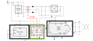
When looking at a use case like the one described here, it’s evident that using a digital isolator also necessitates using an isolated power source. Let’s look at the digital isolator in more detail now.
How Does the Digital Isolator Work?
This is a pin schematic of a standard digital isolator. It has two isolated supplies (VCC1 and VCC2), two grounds (GND1 and GND2), and input and output pins on both sides connected to the relevant grounds. The input signal is modified by a transmit IC before being sent to the receiving side IC via a high voltage capacitive barrier and a connecting bond wire.
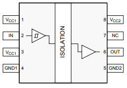
When an input signal is applied, digital inputs and outputs should be equal. As previously stated, digital isolators are most typically employed with isolated power supplies in separate grounds to eliminate ground interference and noise currents from power supplies. CMOS or TTL logic switching technology is used in digital isolators, and they have specific specifications.
The device functional mode part of the datasheet, such as the one shown here, contains the default output states of high or low.
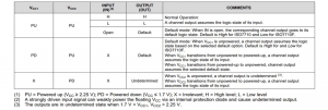
If the inputs are disconnected, or BCC1 is disconnected, the output will transition to a logic state high, as shown in the table. This is referred to as a fail-safe high. In a disconnected condition, some devices will go low, which is known as a fail-safe low. In a supply loss or brownout, this behavior is established to help prevent error codes.
The digital isolators’ logic levels for both supplies, VCC1 and VCC2, can range from 1.8 to 5.5 volts, while some devices may support a wider supply range. Two distinct supply voltages can be employed for each side of the digital isolator because the isolator is based on two separate internal ICs.
We’ll talk about digital isolators’ internal structure and topologies now that we have a high-level grasp of how they work on a functional level.
Why do Digital Isolators Need Isolated Power?
Because each side of the device must have power for both the internal [? die?], and there is no physical link between the two, digital isolators require a separate power supply on the primary and secondary sides. This criterion applies to digital isolators and isolated devices with integrated interfaces, regardless of whether the device provides basic or reinforced isolation.
The supply voltages VCC 1 and VCC 2 determine the digital isolator’s input and output signal voltages. From device to device, the exact relationship to VCC will differ. It is advisable to keep supplies similar to the isolated power supply voltage to guarantee that the output of the digital isolator is optimum for the logic levels of interfacing components.
The MCU signals must operate at 5-volt logic levels when employing a digital isolator powered by 5 volts and interfaced to an MCU. A digital isolator can be powered from a variety of sources.
What Is CMTI and How Does It Affect Digital Isolation?
The maximum tolerated rate of rising or falling of the common-mode voltage applied between two isolated circuits is common-mode transient immunity or CMTI. The two isolated circuits concerning digital isolators are the transmit and receive sides of the isolator, internal to the digital isolator.
When the insulation barrier is impacted by a rapid rise or high fall slew rate for transient, the two internal isolated circuits perform within datasheet requirements, without mistakes. This means that the isolator must be evaluated to ensure that it will function consistently and reliably under a wide range of fast transient activity.
While the CMTI specification isn’t required to meet digital component standards, it is critical to the performance of your design. This is because devices with a low CMTI are more prone to output mistakes and signal failures. As a result, choosing a device with a high CMTI specification is a solid indicator of the device’s dependability in your ultimate use case.
How are Capacitive Digital Isolators Built?
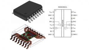
Capacitive digital isolators comprise two independent Integrated Circuit or IC chips—an Input Circuit and an Output Circuit—joined by bond wires and a high-quality, high-voltage resistant mold compound. The digital isolator is illustrated in cross-section and as an X-ray.
A double or single silicon dioxide type of capacitive barrier can be used as the insulator in a digital isolator circuit, and both can resist very high voltage levels by design. The capacitive-based ice is built of the semiconductor industry’s highest dialectic strength type of material. It’s made in a cleanroom wafer fab with low variation from component to part.
The primary contributors to isolation performance are the technology itself and the design architecture due to the tightly controlled manufacturing environment and the quality of the silicon dioxide dielectric. On-Off Keying, or OOK, and edge-based modulation designs were commonly used in capacitive isolators. Both terms refer to the timing strategies that are employed to initiate an output change.
How Does an Edge-Based Isolator Work?
Data transmission is started with an input pulse of a specific duration in an edge-based digital isolator like the one shown below. A high-frequency channel with a bandwidth ranging from 100 kilobits per second to 25 megabits per second and a low-frequency channel with a bandwidth ranging from 100 kilobits per second to DC is the internal data channels in the I/O channel.
A single-ended input signal entering the high-frequency channel is split into a differential signal by the inverter gate at the input. The signal is then differentiated into transient pulses by the capacitor resistor networks. The durations between signal transients are measured by decision logic at the output of the high-frequency channel comparator.
The decision logic compels the output multiplexer to switch from high frequency to low-frequency channel if the delay between two successive transients exceeds a specified time limit, as in a low-frequency signal.
Low-frequency signals are pulse-width modulated with an internal oscillator’s carrier frequency to create a high-frequency signal that can pass through the capacitive barrier. With a time basis typically in the tens of nanoseconds, the oscillator is used to set the timescale of the DC PWM channel. The PWM communication is then packetized, with the smallest packets feasible being higher than the oscillator frequency.
The edge-based isolator is built so that the oscillator frequency does not show up in the output spectrum. Because the input is modulated, a low pass filter is required to separate the high-frequency carrier from the actual data before it is passed to the output multiplexer and output pins, resulting in the electrical isolation of the digital input signal.
How does On-Off Keying Digitize Isolators Work?
The incoming digital bitstream is modulated using an internal spread spectrum oscillator clock with a frequency that operates outside the device’s useful data rate in the OOK or on and off keying architecture. This clock frequency generates OOK signaling, with one of the input states represented by carrier frequency transmission and the other state characterized by no transmission.
On the receive side, which comprises a preamp to gain up the incoming signal followed by an envelope detector, this modulated signal is attached to the isolation barrier and appears in attenuated form. This acts as a demodulator, allowing the original digital pattern to be recovered. The common-mode rejection of the channel is improved by the transmit and receive signal conditioning circuits, resulting in improved Common Mode Transient Immunity, or CMTI.
Which Architecture is Best for My Design?
One of its main advantages is the edge-based modulation system’s lower power profile than the OOK design. The edge-based modulation isolator only enables a signal to pass past the isolation barrier during data transitions or edges; therefore, this is the situation. The OOK architecture, which is continuously sampling and transmitting the modulated input across the barrier, uses substantially less power.
The OOK design consumes substantially more power than the PWM-based edge-based architecture due to the continuous transmission. Are these designs unique in terms of problems and benefits? There are, after all, trade-offs. There is no more sampling of input and output states in the edge-based architecture once a data transmission is established.
This introduces the possibility of an error in the event of a brownout or data signal loss, necessitating an inbuilt refresh circuit to limit the risk of mistakes in these circumstances and reinforce the input state on the output. In the OOK method, continuous input sampling will show no errors at the output in an unplanned supply or input signal change.
The sampling system of the edge-based architecture provides specific power benefits. Additionally, it indicates that the signal conditioning circuits and on-off keying modulation scheme provide intrinsic noise and transient response benefits with substantially greater CMTI and the extra benefit of larger data speeds. So, which capacitive digital isolator topology is better for your application?
When evaluating each architecture, keep in mind the additional design priorities of power vs. data rate, greatest achievable common mode immunity, and management for error circumstances to assist you in finding the optimum fit.
This concludes our overview of digital isolators. Digital ice leads are used to pass digital signals through the isolation barrier and require isolated power and grounds, as we previously mentioned. Silicon dielectric, the industry’s highest dielectric insulation material, is used to produce capacitive isolation. Edge-based and OOK architectures are the two most common capacitive digital isolator architectures.
The output state is the main distinction between edge-based and OOK-based capacitive type of digital isolator designs. Both edge and OOK-based digital isolation solutions have a specified default output high and low state that can be found in the device datasheet. Edge-based systems use the edges of the input stream to generate the output stream after transmitting the data stream through the isolation barrier following an input pulse of a specified length.
And OOK-based solutions, which use a high-frequency carrier to send the data stream across the barrier, allowing for better noise and CMTI performance. Finally, there’s the issue of power consumption. Edge-based systems use less power and transmit data at lower rates, whereas OOK uses more power and transmits data at higher rates.
Conclusion
While digital isolators are designed to work with digital signals, they are routinely used to transfer digitized analog signals. The resulting signal chain will outperform an optocoupler-based system in terms of bandwidth, precision, and linearity. Because optocouplers are nonlinear and have large unit-to-unit variability (+- 50% of your signal), the circuit must be immune to these variations, or each unit must be properly calibrated.
Multiplexing digital channels across a single digital isolator line is a simple process that simplifies the circuit and saves money despite using a more expensive isolation technology. In a nutshell, digital isolators outperform optocouplers in nearly every way. We hope that our comprehensive guide to digital isolators has given you a better understanding of them.
Lastly, if you are looking forward to purchasing digital isolators, we at ICRFQ are the best electronic components distributors in China, contact us today and place your order.
If you want to find more Electronic Components Distributors, check out the following articles:
Electronic Components Distributors In the USA
Electronic Components Distributors In UK
Electronic Components Distributors In China
Electronic Components Distributors In India
Electronic Components Distributors In Singapore
Electronic Components Distributors In Malaysia
Electronic Components Distributors In Vietnam
Electronic Components Distributors In South Korea
Electronic Components Distributors In Taiwan
Electronic Components Distributors In Hong Kong
- Where to buy IC chips? The Best Guide? - March 26, 2024
- Breaking Down Barriers: Overcoming Obstacles in Cross-Border Electronic Component Trade - March 4, 2024
- Everything You Need to Know About Amplifier IC Chips - March 4, 2024


