
Last Updated on July 4, 2022 by Kevin Chen
PCBs, or printed circuit boards, are critical components in the electronic world. They are utilized in everything from simple electronics like toys to essential things like military equipment. Nonetheless, conventional PCBs are typically employed in low-power, low-voltage electronics. This is to make sure things work properly. However, what type of PCB is utilized in devices that require more power and voltage? This article will teach you all there is to know about heavy copper Printed circuit boards. You will learn about heavy copper PCB, its benefits, the production method, and more.
What Is Heavy Copper PCB?
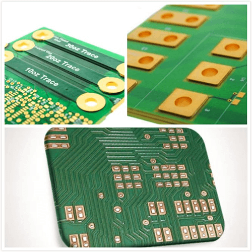
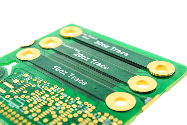
The definition of Heavy Copper boards may not be accurate according to ICP standards, but it won’t be a problem in this case. What a thick copper PCB Design does will be shown to you. A PCB with printed copper conductors typically falls into the heavy copper printed board category. These copper conductors typically weigh between three and twenty ounces / square foot. Between 20 and 200 ounces of copper per square foot are used to make PCBs by some heavy copper Printed circuit board producers. Extreme Copper PCBs is the name given to them in most contexts.
Except for the most popular etching and plating methods, all heavy copper PCB boards employ the same principles. The traditional methods generally included etching a thick copper-clad substrate, which frequently resulted in uneven sidewalls and severe undercutting, in contrast to the current high-speed plating and differential etching techniques.
The Manufacturing Process Of Heavy Copper PCB
There are numerous procedures to think about when producing heavy copper PCBs. However, plating or etching are frequently employed.
Plating or etching aims to provide more copper thickness and plated holes or sidewalls. Heavy copper PCBs, however, call for unique etching and plating techniques. To ensure that the copper is thicker than necessary, do this.
Heavy copper PCB manufacturing is not finished when conventional etching methods are applied. The sole results of conventional etching methods are uneven, over-etched edge lines.
Heavy copper PCBs are electroplated throughout the production process. This aids in making the PCB’s walls thicker.
However, there are some restrictions on the production of heavy copper. For example, the cost of the etching process rises, and a large amount of copper must be removed. Additionally, the surface is uneven due to the dense copper traces.
Benefits of Heavy Copper PCB
It’s evident from the outset of this piece that thick copper boards are often advantageous. You may have already seen some uses for this technology, but let’s start with the advantages:
Compact size
Due to the stacking of previously many layers onto a single layer, heavy copper boards can handle frequency, high temperature, high current, and repeating thermal cycles. This allows for compact, high-performance circuitry while reducing the board’s size and weight.
Multi-use
Any board cannot endure the total weight of the large copper PCB without sacrificing performance or board quality. These boards are more likely to be utilized in conjunction with devices with fluctuating power and signal levels than regular PCB boards.
Resistant to thermal degradation
There is a lot of heat produced by high-frequency boards that the fan cooling system cannot entirely remove. The board’s performance is negatively impacted by this heat, which finally causes the fragile soldered joints to fail. As a result of their improved conductivity, heavy copper PCB boards will not only produce less heat. Still, they will also be significantly more resistant and efficient at dissipating outside heat.
It eliminates the need to have two separate boards
In the past, high-power and control circuits were not commonly seen combined. Control and high-power circuits may now be manufactured on a single board with the help of the heavy copper flex PCB, which enables boards with both high-power and outstanding signal capabilities.
Structural advantage of the board
Because of the layering and plated-through holes, a multilayered heavy copper PCB provides increased mechanical strength.
Better load sharing
Heavy copper combined with copper vias may be employed in place of multiple duplicates and parallel layers (copper-plated). Load-sharing problems caused by several parallel layers are reduced or even eliminated. Along with improving electrical conductivity and heat dissipation, vias improve the performance of heavy copper PCBs.
Applications of Heavy Copper PCB
Due to the advantages and capabilities listed above, heavy copper PCBs are used in various applications. Some examples of these applications are:
Automotive applications
PCBs made of heavy copper is crucial to the automotive industry. To maintain high dependability, automotive PCBs must be lightweight and able to be compacted. They are the best options in this situation due to the advantages of thick copper boards. These characteristics can benefit from air conditioners, Speedometers for cars, GPS navigational devices, telephones, music systems, and security systems.
Other applications could call for a PCB with excellent thermal resistance. In addition to other systems with potentially high temperatures, such applications can be found in the control system, power transmission, and engine system. As low as -40C and as high as 165C are possible for the engine area’s temperatures. These temperature swings can only be securely tolerated by PCBs made of heavy copper (or better).
Heavy copper PCBs have a substantial market thanks to modern electric vehicles. Heavy copper boards’ high-density copper conductors, which are required to manage the charging system’s high current, are insufficient.
Military applications and Aerospace applications
Once more, PCB boards that can survive difficult and harsh conditions are needed by the military and aerospace industries. These situations involve wide temperature variations and a variety of circumstances. Thus, the PCB will have to endure harsh circumstances like the heat of the desert, extreme cold near the poles, and dampness where radar and missile control systems are expected to function. Heavy copper flex PCB at least can withstand all of these circumstances.
The military and aerospace sectors have unique standards regarding equipment production. These are the FR4 Standard PCBs. These criteria require modern etching and plating techniques to keep the edges straight and maintain an ideal etching margin. We have spoken of plating, which involves stacking numerous layers. As a result, the heavy copper PCB will have a smaller layer, lower impedance, and a more compact form while having lower production costs.
Computer applications
Strong hardware that is also more compact than earlier models is required for high-performance computing in the present era. The great conductivity of both current and signals makes copper a common material for computer motherboards.
The UPS is another component of the computer system. A significant amount of high voltage can be used to discharge high currents through UPSs. If this load was applied to a standard PCB, it would heat up, melt certain joints, and short-circuit the board. Thus, a heavy copper PCB must be employed.
Heavy Copper PCB Design Guidelines
Without the required money for the advanced manufacturing process, it might be challenging to produce a heavy copper PCB that is adequate. For heavy copper printed circuit boards to be of the highest quality, criteria are nonetheless being developed over time. Among these suggestions are:
Weight
Utilizing a double layer rather than thicker copper is recommended if the weight is typically anticipated to be greater than 4 oz.
Shape
It could not necessarily be rectangular, depending on how the board is made and its size. This is partially a result of the hefty copper conductors’ potential to alter the board thickness collectively.
Width and thickness
The current carrying capacity mainly determines the width and thickness of the PCB conductor. The highest permissible conductor temperature will also determine the thickness and width.
SMT Pads
Trapezoidal cross sections are created during the etching process. The SMT pad may be considerably smaller than intended, resulting in weaker solder joints and trouble putting components appropriately. To prevent this, multiple solder masks are used to shield the thick copper traces.
Plating is preferred to etching
Making hefty copper boards primarily involves the additive plating and etching procedures (subtractive process). The former is more expensive, but it typically produces superior outcomes.
Merging control and high-power circuits
High-power & control circuits have traditionally been incompatible with one another. Heavy copper plating on the board makes it possible to increase the thickness of copper on the sidewalls to combine the two circuits better. On a straightforward board structure, a high-current board is thus understood.
Thickness tolerance
The usual conductor spacing stays within a +/- 20% tolerance. But the distance between them might be closer.
Extreme copper
The issue of load sharing for the high current over multiple parallel layers can be solved using heavy or extreme copper conductors. Plated-through holes and thick copper vias will then help with conductivity. Thus, a more precise estimation of heat production due to losses on the board is possible. A cooler, more durable board is the end consequence.
Last but not least
The present industrial needs increasingly require heavy copper PCB designs. These PCBs have been used more frequently in the electronics industry, primarily in complex switches that must fit small spaces. Due to copper’s great electrical and thermal conductivity, this is the case. The end product is a multilayered or double-sided board, which may have intricate exterior layers paired with thick copper layers on the interior layers. These boards are so found in planar transformers and power converters.
Conclusion
Heavy copper PCB has many uses and advantages, which have increased demand. They are designed to suit your electrical needs in every imaginable, and you can’t go wrong with them because of their high performance and good thermal conduction and management.
To always work at their best, they will remove heat generated by the conduction of high currents. Therefore, invest in this technology and get the rewards for your electrical application. To get better advice on the hefty copper PCBs, don’t forget to consult an electrical professional.
For more details from designing, manufacturing or bulk purchase of heavy copper PCBs, contact us at ICRFQ. We manufacture the best electrical components in China.
If you want to find more Electronic Components Distributors, please check out the following articles:
Electronic Components Distributors In the USA
Electronic Components Distributors In UK
Electronic Components Distributors In China
Electronic Components Distributors In India
Electronic Components Distributors In Singapore
Electronic Components Distributors In Malaysia
Electronic Components Distributors In Vietnam
Electronic Components Distributors In South Korea
- Where to buy IC chips? The Best Guide? - March 26, 2024
- Breaking Down Barriers: Overcoming Obstacles in Cross-Border Electronic Component Trade - March 4, 2024
- Everything You Need to Know About Amplifier IC Chips - March 4, 2024


