
Last Updated on October 22, 2023 by Kevin Chen
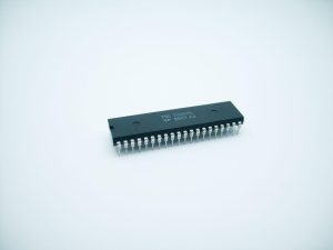
Photo by StudioRemotoNet on Pixabay
Integrated circuits are widely used in electronics nowadays, as they combine multiple electronic functions into a single device. ICs typically have semiconductors as key components and function in digital logic operations. The manufacturing process of an integrated circuit is rather complex, as it involves several steps to complete fabrication of the final product.
Integrated circuit manufacturers also use various tools for each process, so the entire process involves a lot of inspection and testing to make sure every finished product meets standards.
But, how long does the whole manufacturing process take? It is approximated to be between five weeks to eight weeks.
However, the timeframe is likely to vary depending on the technology and tools used by the manufacturer of the integrated circuit.
All ICs have the same general manufacturing process with minor variations based on their size and application.
Each type of IC has its own unique set of challenges for semiconductor manufacturers. Here’s how long it takes to make an integrated circuit:
Determining The Type Of IC
First, you need to determine the type of IC. There are many different types of integrated circuits and many variations of each. For instance, one type of IC may be designed for high-end audio applications, while another may be designed for low-power wireless devices.
Knowing the type of IC to be manufactured will help you to identify the components needed in the circuit. The type of semiconductors used, such as silicon or germanium, is also important, as they have different properties that affect the design.
You also need to consider the amount of power needed and select the right voltage and current rating.
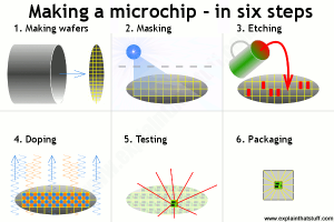
Image source explainthatstuff
Wafer manufacturing
Wafers are made from silicon ingots that are sliced into smaller pieces. Silicon wafers are heated to an extremely high temperature in a special oven and then cooled down, which allows for the ingot to bend without breaking.
Wafer manufacturers use special robots to cut a circular disk from the silicon ingot. Then, the disks are processed in a chemical bath that removes impurities from the wafer.
After the wafer is clean, it is ready to be made into silicon chips. The first step is growing an epitaxial layer on the wafer. Epitaxy is the process of creating a thin layer of single-crystal silicon on top of a silicon wafer with a lower purity.
Deposition
The next process is the deposition of a thin film of metal on top of the silicon wafer. The film acts as a conductor between the silicon and the outside world, allowing electricity to flow through the chip.
The choice of the type of film will vary by manufacturer. For instance, one semiconductor manufacturer may use aluminum while another uses tungsten. Wafer manufacturers use vacuum evaporation to deposit a thin film of metal on the wafer. A vacuum is used to remove any impurities in the air, which will prevent the film from sticking to the wafer.
The metal is melted in a vacuum chamber, and then it is evaporated over the surface of the silicon wafer.
Photolithography
The third process is photolithography, where images are transferred onto the silicon wafer. The images on the wafer will become etched grooves after the wafer is etched. This is necessary to create pathways for the electrical current inside the chip. Photolithography uses a light-sensitive chemical called photoresist to create images on the silicon wafer.
A computer-controlled light pattern is used to draw a circuit pattern on the silicon wafer. The pattern is then transferred to the silicon wafer using a chemical process called etching. A chemical is applied to the silicon wafer that reacts with the photoresist, which allows the chemical to etch away the silicon.
Etching
The holes in the silicon wafer are etched to create pathways for electrical current to flow through the chip. The silicon wafer is placed in a chemical bath, which removes excess silicone while leaving the circuit pattern intact.
The silicon wafer is then rinsed in water to remove the chemicals. The silicon wafer is usually ready for the next process after a few hours or a day.
Thermal processing
This is the process where the silicon wafer is baked in an oven, which melts the silicon and creates the silicon chip.
The silicon is heated to a very high temperature, which melts the silicon and fuses the thin film of metal together with the silicon.
The silicon wafer is baked at very high temperatures for several hours. The silicon wafer is then cooled down to room temperature, and the silicon chip is ready for the next step in the process.
Chemical polishing
The next process is chemical polishing, where excess silicon from the chip is removed. This is necessary to create an even surface and remove imperfections created during the previous steps.
Chemical polishing uses a chemical solution to remove excess silicon from the chip, leaving an even and smooth surface. The silicon chip is placed in a chemical bath along with a pad made of a soft material.
Probe test and final test
In this step the silicon chip is tested with a probe. The probe is held above the silicon chip and touches the surface with tiny prongs.
The probe is connected to a computer, and special software is used to run tests on the silicon chip.
The probe can also be used to apply voltage to the chip, which can simulate the electrical current it will draw when installed in a device. The silicon chip is ready for the last process after the probe test.
The final test is the last process before the silicon chip is ready for the assembly line. The silicon chip is connected to a circuit board to test its functionality and make sure it will operate properly when placed in a larger device.
Assembly and packaging
After the silicon chip pass the final test, the final process is assembly and packaging. The silicon chip is placed on a circuit board along with other components. The components are wires, capacitors, diodes, resistors, and other devices used to control or regulate current flow.
The silicon chip is covered with a material such as epoxy to protect it from the elements and keep it in place. The circuit board is placed in an enclosure and connected to a power source. The finished product is then tested and ready for shipping to end users.
Conclusion
Now you know what it takes to manufacture integrated circuits. It is an elaborate process that ensures that at the end of the day you have a fully functional chip.
Reputable IC distributors and sourcing agents such as ICRFQ source their ICs from reputable manufacturers that follow all these processes.
You can be sure of getting quality integrated circuits from such distributors in China.
If you want to find more Electronic Components Distributors, please check out the following articles:
Electronic Components Distributors In the USA
Electronic Components Distributors In UK
Electronic Components Distributors In China
Electronic Components Distributors In India
Electronic Components Distributors In Singapore
Electronic Components Distributors In Malaysia
Electronic Components Distributors In Vietnam
Electronic Components Distributors In South Korea
- Where to buy IC chips? The Best Guide? - March 26, 2024
- Breaking Down Barriers: Overcoming Obstacles in Cross-Border Electronic Component Trade - March 4, 2024
- Everything You Need to Know About Amplifier IC Chips - March 4, 2024


