
Last Updated on October 22, 2023 by Kevin Chen
In recent years, integrated circuit substrates have gained popularity. It has arisen as a result of the introduction of integrated circuit types such as the chip-scale package (CSP) and the ball grid package (BGP) (BGP). Novel package carriers are required for IC packages, which the IC substrate considers. Understanding the relevance of the IC package substrate as an electronics designer or engineer is no longer enough. You must be familiar with the IC substrate production process, the role that substrate ICs play in the proper operation of electronics, and its various applications.
What is IC Substrate
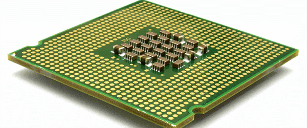
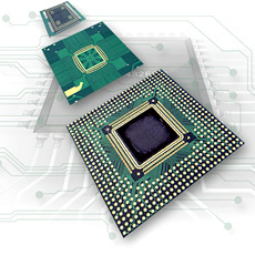
A bare integrated circuit chip is packaged on an IC substrate, a baseboard form. The substrate IC serves as a link between the chip and the circuit board. Integrated circuits are a transitional product that includes a semiconductor integrated circuit chip, routing to connect the chip to the PCB, and safeguarding, supporting, and reinforcing the IC chip to provide a thermal dissipation tunnel.
The integrated circuit substrate serves as the link between the printed circuit boards and the semiconductor chip. It serves as a conduit; thus, IC fabricators must have enough capacity to deliver higher connectivity densities than PCB fabricators during the IC substrate fabrication process. As a result, manufacturers will need to have demonstrated understanding and solutions in chemical expertise for high-density designs.
Integrated circuit substrates come in various shapes and sizes, and they are classified differently. We’ll look at each categorization and the numerous varieties inside each class to better understand everything.
Integrated Circuit Substrates Classification by Packaging Types
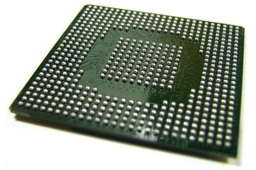
BGA stands for Ball Grid Array. It’s an IC substrate with good electrical and thermal dissipation characteristics. It is suitable for integrated circuit packages with pin counts above three hundred since it may dramatically increase chip pins.
Integrated Circuit Substrate (CSP) is a substrate used to build integrated circuits. It’s a small, single-chip package. The CSP IC substrate is primarily used in low-pin-count telecommunications and memory applications.
FC Integrated Circuit Substrate is an acronym for “Fibre Channel Integrated Circuit Substrate.” Low circuit loss, low signal interference, and effective and efficient thermal dissipation are all features of the flip-chip type packaging.
MCM Integrated Circuit Substrate is a type of integrated circuit substrate. Multi-chip module is the abbreviation for “multi-chip module.” It’s an integrated circuit substrate that absorbs chips that execute several functionalities in a single package. As a result of its thinness, lightness, miniaturization, and brevity, the product is a perfect answer. Because numerous chips are bundled into one, this substrate type cannot perform well in terms of thermal dissipation, signal interference, precise routing, etc.
Classification by material characteristics
Substrate for Rigid Integrated Circuits. ABF resin, BT resin, or epoxy resin are the most common components. It has a thermal expansion coefficient of around 13-17ppm/°C.
They have integrated Circuit Substrate with Flexibility. The primary elements of the IC substrate are PE or PI resin, with a CTE of 13-27ppm/°C.
Ceramic Substrate for Integrated Circuits. Ceramic materials such as aluminum nitride, aluminum oxide, and silicon carbide are used. The CTE of the ceramic IC is comparably low, ranging from 6 to 8 ppm/°C.
Classification by bonding technology
- Tape Automated Bonding (TAB)
- Wire Bonding
- FC Bonding
While the significance of the IC substrate cannot get overstated, it is impossible to discuss it without mentioning IC packaging. It’s important to remember that it’s one of the most common integrated circuit substrate classifications.
The material that houses the semiconductor device is referred to as IC packaging. It protects the IC substrate from physical damage and corrosion while also enabling the installation of electrical connectors. It’s particularly important to connect the electrical contacts to the PCB. Integrated circuit packaging solutions come in a variety of designs. It’s crucial to think about these different sorts because they all have different requirements for their outer shells.
What Is IC Packaging?
The material that houses a semiconductor device is known as IC packaging. The package is a casing that protects the circuit material from corrosion and physical damage while also allowing electrical connectors to link it to the printed circuit board to be mounted (PCB). There are many various types of integrated circuits. Thus, different IC packaging system designs are to consider, as each circuit design will have varied needs for its outer shell.
Why Is IC Packaging Important?
In the fabrication of semiconductor devices, IC packaging is the final step. The semiconductor block is encased in a package during this crucial stage, which shields the IC from potentially harmful exterior elements and the corrosive effects of time. The package is simply an encasement that protects the block while promoting the electrical contacts transporting signals to an electronic device’s circuit board.
Since the 1970s, when electronics packaging makers initially used ball grid array (BGA) packages, IC packaging technology has advanced. Newer packaging technologies, such as the plastic quad flat pack and the thin small outline package, supplanted pin grid array packages at the turn of the century. The Land Grid Array Packages Era was ushered in by manufacturers such as Intel as the decade progressed.
Meanwhile, BGAs were phased out, favouring flip-chip ball grid arrays (FCBGAs), which had a higher pin-count than other package types. Instead of only the edges, the FCBGA has input and output signals around the die.
IC packaging designs
Different classifications exist for IC packaging designs based on their creation. The substrate type and the lead-frame type are both included. You will find the following information here.
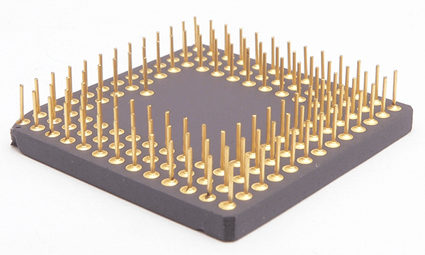
- Pin-grid array. It gets deployed in socketing.
- Dual-inline and lead-frame packages
- These packages are utilized in assemblies where pins must pass through holes.
- Chip scale package. It’s a single-die package that can be directly surface mounted. It has a small area about 1.2 times smaller compared to a die)
- Quad flat pack that is a leadless package but with a frame.
- Quad Flat with no-Lead but with a tiny package which resembles a chip size and is primarily deployed for surface mounting.
- Multichip package. The package, also known as multichip modules, combines discrete components, semiconductor dies, and several ICs onto a single substrate. As a result of this configuration, it becomes a multichip package and resembles a larger IC.’
- Package for creating area arrays. It’s a type of packaging that maximizes performance while conserving space by interconnecting any remaining portion of the chip’s surface.
It’s worth noting that most businesses use area array packages like the BGA. It occurs as a result of the requirement for multichip structures. These packages and modules are superior to solutions based on the system-on-chip format.
Applications of Integrated Circuit Substrate PCB
IC substrate PCB is mostly used in the manufacture of specialized electrical products. These products must be thin, light, and offer advanced functions. As a result, IC substrate PCBs can be found in medical care, telecommunication, aerospace, industrial control, and the military on smartphones, tablet PCs, laptops, and networks. The most common application is a mini-led PCB, while micro led is also an IC substrate application.
Over time, most rigid printed circuit boards have evolved from multilayer PCBs to substrate-like PCBs, or SLPs, to classic HDI printed circuit boards to integrated circuit substrate PCBs.
Features of an Integrated Circuit
A precise set of qualities must be present in an IC substrate to align with the features of an integrated circuit. Electronic engineers and designers must understand the characteristics of an integrated circuit to choose the appropriate IC substrates when building integrated circuits. So, what are some of the most important IC characteristics?
- Circuit of a small size. Because integrated circuits are typically downsized, the design, installation, and debugging processes must be consistent and straightforward.
- Cost-effectiveness. All integrated circuits frequently have superior performance and lower costs than discrete components.
- Integrated circuits are extremely dependable, thanks to a lot of effort to improve their reliability, particularly performance and consistency. In integrated circuits, soldering joints are considerably reduced. In addition, virtual welding is no longer required, making the IC even more dependable.
- Lower the risk of failure. When compared to traditional circuits, integrated circuits have a lower failure rate.
- Energy-efficient. Integrated circuits are also energy efficient since they use less energy or power, are produced in smaller quantities, and cost less.
These characteristics are also some of the most important advantages of integrated circuits. It does not, however, end there. Particular attention should be paid to the properties of the IC substrate while designing the IC for your electronic product.
Attributes of an IC Substrate
Integrated circuits contain a wide range of capabilities. It contains the following items.
- It is lightweight.
- Fewer soldered joints and lead wires
- Exceptionally dependable
- Performance improves when other factors like reliability, durability, and weight are considered.
- Small size
Manufacturing Process of IC Substrate PCB
The integrated circuit substrate is the basic connection between a printed circuit board and an IC chip. This is achieved using a network of conductive traces and holes. But what does an IC substrate manufacturing process entail?
Manufacturing Steps
- Patterning and Plating of Copper.
The production process is the initial phase. It involves copper plating and patterning, linked to various technological factors such as circuit and control compensation, Uniform Copper Plating Thickness Management, and fine-line manufacturing.
- Mask for Soldering.
It is made in the same way that copper is patterned and plated. Hole filling and solder mask printing procedures for integrated circuit substrate PCBs make up the solder mask. IC substrate PCBs have consistently allowed a substrate height difference of less than ten micrometres between solder mask and pad. More than fifteen micrometres, on the other hand, is not recommended.
- Finishing the Surface.
It is critical to establish a uniform thickness of the surface finish in this step. It entails using ENEPIG and ENIG surface treatments, which are widely accepted.
- Inspections and testing for dependability is the final step in producing an IC substrate.
The integrated circuit substrate must be verified for dependability and evaluated for quality assurance. The technology used in testing dependability and inspection, on the other hand, differs from that used in regularly printed circuit boards.
Despite the processes stated above, it is important to recognize that the manufacturing process of integrated circuit substrate PCB is not simple. We’ll take a closer look at the many technologies involved in the fabrication or manufacturing process to put everything into context.
Technologies Involved in the Integrated Circuit Production Process
In every stage of the IC manufacturing process, a wide range of advanced technologies is used. Manufacturers can use the technologies to assure high-quality, high-capacity, high-precision connectivity products for progressive IC packaging while lowering costs and increasing productivity.
Direct Imaging Systems
The FCBGA (flip-chip ball grid array), FCCSP (flip-chip chip scale package), module, and BGA/CSP (ball grid array/chip scale package) applications are among the most complex that the direct imaging technology solution can handle. As a result, fabricators or manufacturers can achieve higher yields while lowering their total cost of ownership (total cost of ownership).
The technology provides unrivalled outcomes, such as fine-line imaging down to around 8m and higher and faster throughput registration accuracy. The modified semi-additive process and semi-additive process, as well as other unique substrate processes, are supported by such established systems.
Some of the applications are fine-line direct imaging of plate-resist and etch-resist FCBGA), FCCSP, and BGA/CSP.
Automated Optical Inspection Systems
High throughput and high-resolution inspection are both possible with an automated optical inspection. It uses a solo scan to inspect the integrated circuit substrate panel using many light sources. As a result, it provides unrivalled detection precision and manufacturing efficiency.
Fine inspection patterns with FCCSP and FCBGA integrated circuit substrates is one of its applications.
AOS or Automated Optical Shaping Systems
The AOS offers several options for shaping short faults in top-of-the-line integrated circuit substrate boards to the highest possible quality. The process of precisely molding intricate or fine panel faults that would otherwise be scrapped allows integrated circuit substrate makers to increase yield while lowering scrap significantly.
As a result, high volumes of high-quality boards are ensured. This is a fully automated, user-friendly procedure with high throughput. As a result, it provides significant cost reductions in staffing and a low total cost of ownership (total cost of ownership). It’s used in the AOS of short faults in integrated substrates like FCGBA and FCCSP.
UV Laser Drilling Systems
The ultraviolet laser drilling capability answers some of the most difficult integrated circuit substrate application questions. Aside from output yield, it provides exceptional performance. The UV-laser drilling equipment has an exceptional beam quality, 6m precision, and a fine through the size of 20m diameter.
As a result, it’s perfect for FCBGA and other sophisticated integrated circuit substrate applications. It’s also been improved to enable advanced packaging applications, including embedded die, organic interposers, and LTCC (low temperature co-fired ceramic). It is primarily used in embedded dies, FCBGA, and LTCC to drill through-hole and blind vias.
Inkjet or Additive Printing Systems
The technology provides great precision, productivity, and print quality at a low total cost of ownership. Its goal is to use design to print dams for FCCSP, BGA, and SiP (advanced system in package) modules. As a result, fabricators can save money and space by placing a protective barrier to block off the adjacent die region and prevent underfill leakage.
Selective insulation layer printing is also possible on the QFN (quad flat no-lead) package, an integrated circuit substrate, etc. As a result, it removes the expensive lithography phases, streamlines the traditional process, and reduces operational costs. It also allows for a faster ramp-up and time to market for fresh or new products.
For 2D and legend barcode package marking, additive printing systems technology offers a clever and safe CAM-ready (computer-aided manufacturing) alternative. These indications eliminate the possibility of harm from contact or heat. It delivers perfect pattern alignment, high contrast, high speed, fine-featured printing, and accurate and uniform material deposition on complicated and uneven surfaces.
Design Consideration for Integrated Circuits
It helps to understand and examine the different technical factors of the integrated circuit design if you want to choose the best IC package or IC substrate. Knowing the correct material composition and substrate for your integrated circuit package is an example.
It’s also crucial to understand the distinction between the tape and the rigid package substrate. Other companies, particularly those that work well with metal conductors, choose laminates as substitutes for substrates and lead frames. So, what aspects of design should you concentrate on?
Material Composition
An integrated circuit’s electrical, chemical, material, and electrical constitution significantly impacts its performance. While laminate packages and lead frames serve different purposes, they rely on the same material composition. The most common package format is lead-frame, which uses gold or silver wire-bond finishes connected via spot plating. It makes the process easier and more economical.
Alloy 42 is commonly used as the metal type in ceramic packages because it works well with the core material. On the other hand, plastic packaging favour copper lead frames to protect the solder junction while also providing conductivity. Material consideration as a critical factor for SM (surface mount) plastic containers is encouraged in some countries.
The lead finish has been exposed to severe examination regarding the next-level packaging assembly due to frequent modifications of European regulations. It arose from the necessity to find suitable substitutes for tin-lead solders, which are easy to use and have become an industry standard. On the other hand, Fabricators have failed to unite around a single solution due to fierce rivalry. As a result, the leading question appears to be one that will remain unanswered for some time.
Laminates have been a feasible alternative to lead frames in chip-to-board assemblies since the 1970s. Laminates are widely used in the integrated circuit packaging solutions sector due to their significant cost savings over ceramic substrates. The top and most prevalent laminates are still high-temperature and organic substrates. Aside from being cost-effective, these laminates have exceptional electrical properties.
Applicable Substrates
The popularity of semiconductor packages has increased the demand for appropriate interposers and substrates. A substrate is an essential component of an integrated circuit package, as it provides mechanical strength and allows the board to communicate with external components and devices. The interposer, on the other hand, allows for package-wide connective routing. It’s also worth noting that the phrases “interposer” and “substrate” are sometimes used interchangeably.
Difference Between Tape and Rigid Package Substrates
Package substrates are frequently available in tape or rigid forms. Rigid substrates are strong and have a fixed shape, whereas tape substrates are thin and flexible. In terms of composition, integrated circuits used to be made of ceramic material, but now they are made of the organic substrate material.
A laminate substrate is inferred if a substrate has a stack of many thin layers that result in a hard substrate. Bismaleimide-triazine (BT) and FR-4 are the two most common and standard laminate substrates used in integrated circuit production. The FR-4 is made of epoxy, but the BT is made of a high-grade resin.
The low dielectric constant and insulating properties of BT resin have made it a popular choice. When it comes to BGAs, BT is used in practically every other substrate. It also works well as a resin for CSP laminates (chip scale package) laminates. On the other hand, many industrial companies are developing new epoxy mixes and alternatives to give BT a run for its money. The conclusion of this competition could result in a price reduction.
Tape substrates are a great substitute for rigid substrates. Polyimide and other temperature-tolerant and durable polymers make up most of the material. The ability of tape substrates to carry circuits while moving is one of their advantages. As a result of its versatility, it’s a common choice for mobile devices like disk drives. Furthermore, tape substrates are light in weight, ensuring that the surface is placed on is not burdened.
Substrates Designed to Assist Metal Conductors
Metal wires capable of routing signals to various linking features should be included in integrated circuit packages. As a result, the substrate must make the procedure easier. The chip’s output and input signals are frequently routed to various features in packages via substrates. Copper, commonly the placement foil, is bonded to the substrate’s laminate to achieve metal conductivity. Nickel or gold immersion coatings are applied on copper to avoid oxidation and inter-diffusion.
Conclusion
IC substrates are critical for connecting the PCB and the IC chip in electronics. As a result, knowing everything about them can mean the difference between a successful or flawed IC design for your electronic application. As a result, keep the points listed in mind when developing your IC for a better result.
Lastly, you can also contact us ICRFQ; we are the best manufacturers of IC and other electrical components in China.
If you want to find more Electronic Components Distributors, please check out the following articles:
Electronic Components Distributors In the USA
Electronic Components Distributors In UK
Electronic Components Distributors In China
Electronic Components Distributors In India
Electronic Components Distributors In Singapore
Electronic Components Distributors In Malaysia
Electronic Components Distributors In Vietnam
Electronic Components Distributors In South Korea
- Where to buy IC chips? The Best Guide? - March 26, 2024
- Breaking Down Barriers: Overcoming Obstacles in Cross-Border Electronic Component Trade - March 4, 2024
- Everything You Need to Know About Amplifier IC Chips - March 4, 2024


