
Last Updated on October 22, 2023 by Kevin Chen
Image Source: Siemens EDA
Integrated circuit (IC) design is a complex, multifaceted process that requires specialized software to complete.
There are several different types of software out there, each with its own set of benefits and limitations.
Depending on your specific needs, you’ll want to choose the right software for the task at hand. Integrated circuit design involves a series of highly-specialized functions, from schematic capture to physical layout and everything in between.
To get started, it’s helpful to understand all the different kinds of software available and how they interrelate with one another.
Software can appear complicated at first glance, but once you understand the basic principles behind each kind, it becomes much simpler.
Key reasons for using software to design IC
If you’re designing a complex circuit or product, chances are you’ll need to use some sort of software. There are a number of reasons why. Here are 5 reasons software is essential for IC design:
Improved productivity
Designing circuits with software is faster and more efficient than manual design. Designing with software allows you to iterate on your design much faster than a manual approach, enabling you to get to a final design much more quickly.
Increased design quality
When you design with software, you’re able to explore more design options. This lets you more easily design for functionality, yield, and testability.
More accurate design
Designing with software is more precise than a manual approach. It’s much easier to work with tolerances when using software, helping you to avoid costly design mistakes.
Better collaboration
Designing circuits with software enables you to better collaborate with your team members on the project, ensuring a smoother design process. You’re able to share your design with others, track their progress, and keep everyone in sync.
Overview of software used in IC design
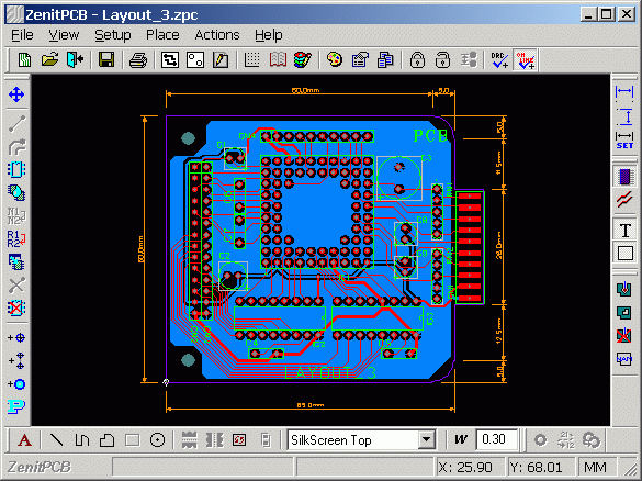
Image source electroschematic
There is a wide variety of software applications that are used in designing integrated circuits. Let’s look at some of them and what they do.
CAD and CAM Software
CAD and CAM software are the most common types of software for integrated circuit design.
These types of software are used for both analog and digital circuits, and they help you to create a schematic diagram and related files. CAD and CAM software can be used to create schematics, PCB layouts, and part drawings. It’s important to note that CAD and CAM software are not design automation (or design) tools.
Design tools are used for the actual design process itself, whereas CAD and CAM software are used for the prep work. CAD and CAM software are used to create a schematic and PCB layout. You can then use the same schematic and layout files to drive the design tools that are used to design your circuit.
Electronic Design Automation (EDA) Software
EDA software is the ultimate design automation tool. It’s an end-to-end design tool that includes schematic capture, layout, and simulation functionality. EDA tools are specialized software tools that are typically used by engineers when they need to design complicated chips.
There are many different types of such tools available, each with its own set of benefits and limitations.
For example, there are analog EDA tools and digital EDA tools. Digital EDA tools are used to design circuits that include both digital and analog components.
Digital EDA tools can also be used to design mixed-signal circuits, which are circuits that include both digital and analog components but also have some specialized digital components.
Physical layout software
Physical layout software is used to define the physical locations of components on a printed circuit board (PCB).
Physical layout software is used in conjunction with CAD and CAM software. With CAD and CAM software, you create a schematic diagram and a PCB layout drawing. Physical layout software allows you to identify the physical locations of components on a PCB.
It’s important to note that physical layout software doesn’t actually create a PCB layout. Rather, it simply defines the locations where components will be placed on a PCB.
Electronic layout software
Electronic layout software is almost identical to physical layout software. The main difference is that electronic layout software allows you to specify the electrical properties of each component.
Electrical properties include things like impedances, capacitances, inductances, resistance, and voltage drop. Unlike physical layout software, electronic layout software doesn’t take into account things like trace width and spacing.
Electrical layout software is used to design Printed Wiring Boards (PWBs) and Printed Circuit Boards (PCBs). A PCB is an electronic circuit that’s constructed on a flat surface. A PWB is a PCB that’s been cut up into smaller pieces that can be used in different parts of a circuit.
Electrical layout software allows you to create circuit boards that are capable of functioning as intended. It’s important to note that electrical layout software doesn’t actually create the PCB layout. Rather, it simply defines the locations where components will be placed on a PCB.
Schematic capture software
Schematic capture software is used to create circuit diagrams and is usually the first software you’ll use in the design process.
You’ll also use schematic capture software to create your initial schematic. This initial schematic is then used to create other files, such as a PCB layout, a PWB layout, and an electrical layout.
One of the key benefits of schematic capture software is that you can use it to create an electronic design that can be used for both digital and analog circuits.
While you can also create a digital design with an analog EDA tool, schematic capture software is more flexible and easier to use.
Mixed-Signal Simulation Software
Mixed-signal simulation software is used to simulate the operation of circuits that contain both digital and analog components.
It’s important to note that mixed-signal simulation software isn’t used to design the circuit.
Instead, it’s used to test the circuit once it’s been designed.
Mixed-signal simulation software is used to test both digital and analog parts of a circuit. This software allows you to see how the circuit will operate in real-world conditions.
Overview of IC design process
To understand what the software do, let’s have a brief overview of the integrated circuit design process. You will then appreciat the role that these software tools play in the creation of the final product.
Conceptual stage
The conceptual stage encompasses all activities related to the idea behind the design. This includes everything from determining the product requirements to specifying the manufacturing process and the layout and architecture of the chip. This is the stage where you might use Mathematica’s intellectual tools to simulate different design alternatives.
For example, you can use systems modeling to determine the optimal architecture for your design, given a set of specified requirements. In other cases, you might use differential equations to model the timing of the design, again given certain specific parameters. Different types of design tools can help with architectural and layout design.
Architectural design
The architectural design phase is all about making the logical design fit within the physical architecture of the chip.
Typically, this involves deciding on the number of cores, the interconnection network (timing and routing), and the placement of the modules, along with their relative position to one another.
An EDA tool like Cadence’s Alliance Customizable Design Environment (CADE) can help you to design the architecture of your chip. CADE offers a wide range of architectural and timing options for designing the interconnects between modules. After the architecture is finalized, you will move on to the logical design phase, where you will specify the functionality of each module.
Logical design
The logical design phase is where you actually specify the functionality of each module and the connections between them. This is where you get down to the nitty-gritty details of your design.
This is where you will want to use an EE IDEs like Mentor’s Design Core, which offers a wide selection of implementation tools. You can use the tools to specify how you want each module to function and how you want it connected to the rest of the design.
You may also want to use an advanced language like SystemVerilog or VHDL to specify the functionality of each module. A SystemVerilog simulation environment can help you to test and debug your design.
Circuit design
The circuit design phase is where you actually create the layout of the individual modules. You will have already specified the functionality of each module during the logical design phase and connected them to each other.
Now it is time to determine the actual placement of the various components. In a general-purpose layout tool like Mentor Graphics’ Frontier or Cadence’s Logic Schematic and Design Automation (LSDA), you will specify the actual physical parameters of each module, such as the number of gates, the interconnections, and the actual placement on the chip.
In the past, you would have used special-purpose circuit design tools for this task. However, since the advent of EDA tools, the majority of circuit designers now use an EE tool for layout.
Physical Layout
The physical layout phase is when you actually create the final layout of your design. The circuit design tools mentioned above will create a physical layout of your design by determining the exact placement of all the components on the chip. This includes routing the interconnects between the modules.
The tools will also create a parasitic overlay, which is basically a map of the power consumption of your design.
This is important when you are considering the power budget of your design. Most of the tools also provide a netlist, which is basically a list of all the connections in the design. This is important for the subsequent steps of the design process.
Verification of the design
The verification of the design phase is when you check that the design actually does what it is supposed to do. This is one of the most important steps in the design process, so make sure you don’t miss it out.
A good design verification flow will include a combination of simulation, formal verification, and functional verification. A system-level simulator like Mentor’s Questa or Cadence’s Concordia can help you to verify the functionality of the design at the system level.
A formal verification tool like FormalCore or Rewired can be used to verify the design at the gate level. A functional verification tool like TestXcell can be used to create test vectors and test the design at the system level.
Sign off
Finally, when you have verified the design and all the necessary parties (e.g., the customer, the manufacturing engineers, the procurement team, etc.) are satisfied, you can move on to the sign-off phase.
The sign-off phase is when you finalize the design and proceed with putting it into production. You will send the design files to the vendor and get the final masks. You will also send the design files to the EDA vendors, who will create the design rule check (DRC) files.
The DRC files are used by the EDA tool to check for gross design rule violations (such as exceeding the allowed maximum length for a net).
When you go into production, it is important to make sure you have all the necessary documentation for the design.
This includes the schematic, the netlist, and the layout. You may also want to create a design report, which is basically a document that details the design decisions that you have made.
Which IC design Software is Right for You?
Depending on your specific needs, you may need to use different pieces of software at different stages of the design process.
Due to the interrelationship between the different types of software, you may even use multiple pieces of software simultaneously.
Choosing a reliable IC supplier in China
When choosing an IC supplier in China, it’s important to select a supplier with a good track record.
A supplier with a strong reputation will have a proven track record for meeting customer needs, providing excellent service, and adhering to a strict code of ethics.
The best way to determine the reputation of an IC supplier is by reading online reviews from customers who have previously ordered from them.
Also, you’ll want to find a supplier who can meet your specific design requirements.
There are many things to consider when choosing an IC supplier, such as design expertise, key services provided, shipping terms, and payment terms.
ICRFQ is one of the suppliers in China that meet all these requirements. We specialize in distributing perfectly-designed integrated circuits for sale.
If you want to find more Electronic Components Distributors, please check out the following articles:
Electronic Components Distributors In the USA
Electronic Components Distributors In UK
Electronic Components Distributors In China
Electronic Components Distributors In India
Electronic Components Distributors In Singapore
Electronic Components Distributors In Malaysia
Electronic Components Distributors In Vietnam
Electronic Components Distributors In South Korea
- Where to buy IC chips? The Best Guide? - March 26, 2024
- Breaking Down Barriers: Overcoming Obstacles in Cross-Border Electronic Component Trade - March 4, 2024
- Everything You Need to Know About Amplifier IC Chips - March 4, 2024


