
Last Updated on October 22, 2023 by Kevin Chen
The digital interface is often the limiting factor for throughput as data converter rates grow. The current serial standard, JESD204B, from the Joint Electron Device Engineering Council (JEDEC), is constrained by lane speed and wasteful 8B/10B coding. This is addressed in JESD204 revision C, but what does this mean for board layout and protocol implementation? I’ll describe the distinctions between the JESD204 B and C standards, as well as the implications for engineers working on high-speed data converter board designs, in this article.
The requirement for a consistent way for serializing data-converter digital data and reducing the number of interconnects between mixed-signal devices and a processing unit such as a field-programmable gate array prompted the development of the JESD204 interface standard (FPGA). The standard has gone through various versions, with the B version being one of the most well-known and widely used. However, given the demand for even quicker data converters, the existing version loses steam. New device releases like the Texas Instruments ADC12DJ5200RF breach the 10-GSPS barrier and adopt the C standard to keep up with the required throughput.
For those who have studied the JEDEC documents, JESD204 may appear difficult. Nonetheless, the standard was created to deal with the massive volumes of data generated by current mixed-signal devices, including analog-to-digital converters, digital-to-analog converters, and analog front ends.
History of The JESD204 Interface Standard
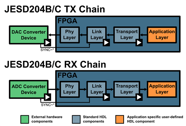
The A standard, which could not synchronize numerous collocated devices, was succeeded by JESD204B. In other words, if you needed the inputs (or outputs) of two identical data converters on a circuit card assembly to be phase-coherent, you couldn’t utilize the A standard because it didn’t allow any way of doing so. Sub-classification was introduced in the B standard, with a backward-compatible mode (subclass 0) and two additional classes (1 and 2) that offered deterministic latency between sampling time and data receipt in the consumer (such as an FPGA). The JESD204A revision was significantly slower than the B revision. The initial standard allowed for a maximum line rate of 3.125 Gbps, but the B standard allowed for a lane rate of up to 12.5 Gbps. As the lane rates grew, signal integrity, clock recovery, and baseline wander were prevalent concerns with high-speed serial communications. An unbalanced quantity of 1s and 0s on a transmission line causes the dielectric to charge, and the transmission line’s DC center point to move, creating baseline wander. This movement can result in two major problems: jitter and coding mistakes. The most typical cause of baseline wander in AC-coupled systems is compensating DC offsets between the transmitter and receiver.
The original standard used 8B/10B symbol encoding to reduce baseline drift and provide AC coupling. A simple lookup table returns a 10-bit “symbol” for each octet for those unfamiliar with this form of coding (8-bit word). Other creative solutions to overcome the running discrepancy of 1s and 0s and maintain a stable DC point on the line while always supplying transitions to bridge-coupling capacitors are introduced by 8B/10B symbol encoding.
Some extra symbols are utilized for in-band signaling to the receiver rather than data transmission. The K28.5 (comma) symbol, for example, is used for lane alignment so that the receiver knows where the bits begin in the stream when it first starts up (for instance, to locate the beginning of a symbol frame). Once the receiver has established a connection, it can announce to the encoder (through the SYNC signal) that it matches the encoder, allowing data transfer to commence.
Although 8B/10B coding is a great way to serialize and deserialize data, it reduces each lane’s capacity by 20%. (channel). As a result, 10 bits are transmitted for every 8 bits provided by the sender (see Figure 1 as an example). Coding 8B/10B becomes increasingly wasteful as data capacity grows.
What’s New in JESD204C?
The C revision of the standard has numerous improvements, improving coding efficiency and overall throughput. The JESD204C standard is backward compatible with the A and B standards; however, the subclass-0 operation is limited. Designers familiar with the JESD204B revision will notice compatibility based on the coding scheme and recommendations for higher throughput utilizing standard upgrades.
The addition of denser 64B/66B and 64B/80B coding schemes is the most noticeable difference; these methods are significantly more efficient in symbol coding. The coding overhead for 64B/66B is only 3.125 percent, compared to 20% for 8B/10B. The disadvantage is that the higher symbol length takes longer to encode at first, resulting in coding latency because most data converters only deliver 8 to 16 bits of data per sample.
Since the B revision, little has changed in the 8B/10 B revision. All of the subclasses 0, 1, and 2 are supported. Subclass 0 is the A revision’s backward-compatible mode, which is utilized to achieve the shortest link delay achievable without deterministic latency. The first and second subclasses define deterministic channel latency and multi-device phase alignment. The transport uses the SYNC interface and the initial lane alignment sequence (ILAS) to establish data alignment and channel latency.
The JESD204C 64B/66B and 64B/80B coding standards are more complex, and they no longer rely on the ILAS and SYNC interface to ensure accurate frame alignment. Instead, these modes employ a SYNC header, which is included in the first two bits of every frame and concatenated into a 32-bit SYNC message. The sync header symbol (2 bits – 01 or 10 are permissible sync symbols, 00 and 11 are unlawful values) is encoded into the SYNC header stream at the start of every 66-bit run.
A pilot signal is always present in this stream, which is needed for 66-bit frame sync alignment. Blocks are made up of multiple frames, and extended multi-blocks comprise groups of blocks. After determining where the SYNC is located in the stream, the receiver proceeds to determine where the frames are aligned by using the last frame indicator to sync to the frame boundaries.
Aside from coding, several novel types of data transmitters and receivers are helping to improve transmission speed and reduce interface power. Table 1 depicts these classes.
| Table 1. | |||
| Device Class Category | Device Class | Additional Comments | Supported Data Rates |
| B | B-3 | 0.3125-3.125 Gbps | |
| B | B-6 | 0.3125-6.375 Gbps | |
| B | B-12 | 6.375-12.5 Gbps | |
| C | C-S | Short-reach channel class | 6.375-32 Gbps |
| C | C-M | Medium-reach channel class | 6.375-32 Gbps |
| C | C-R | Reflective channel class | 6.375-32 Gbps |
Conclusion
Engineers working with JESD204C interfaces can now use a variety of additional modes of operation to synchronize numerous converters and boost the digital interface’s performance. The additional procedures to establish a C-compliant interface should not be demanding for individuals familiar with JESD204B; if the signals are used, a bring-up mode in 8B/10B might simplify development. Once the interface is operational in 8B/10B, you can use higher coding and lane rates to maximize the data converter’s performance.
If you are looking forward to purchasing JESD204B OR JESD204C in bulk, we at ICRFQ are the best electrical components manufacturers in China. Contact us today.
If you want to find more Electronic Components Distributors, please check out the following articles:
Electronic Components Distributors In the USA
Electronic Components Distributors In UK
Electronic Components Distributors In China
Electronic Components Distributors In India
Electronic Components Distributors In Singapore
Electronic Components Distributors In Malaysia
Electronic Components Distributors In Vietnam
Electronic Components Distributors In South Korea
- Where to buy IC chips? The Best Guide? - March 26, 2024
- Breaking Down Barriers: Overcoming Obstacles in Cross-Border Electronic Component Trade - March 4, 2024
- Everything You Need to Know About Amplifier IC Chips - March 4, 2024


