KSP2222A
Part Number: KSP2222A
Manufacturer: Fairchild Semiconductor
Description: General Purpose Transistor
Shipped from: Shenzhen/HK Warehouse
Stock Available: Check with us
ICRFQ.com - Electronic Components Distributor in China Since 2003

We make your sourcing easier!
Get A Fast Quote Worldwide!

Part Number: KSP2222A
Manufacturer: Fairchild Semiconductor
Description: General Purpose Transistor
Shipped from: Shenzhen/HK Warehouse
Stock Available: Check with us
| Datasheet | |
|---|---|
| Category | Discrete Semiconductor Products |
| Family | Transistors – Bipolar (BJT) – Single |
| Manufacturer | Fairchild Semiconductor |
| Series | – |
| Packaging | Bulk |
| Transistor Type | NPN |
| Current – Collector (Ic) (Max) | 600mA |
| Voltage – Collector Emitter Breakdown (Max) | 40V |
| Vce Saturation (Max) @ Ib, Ic | 1V @ 50mA, 500mA |
| Current – Collector Cutoff (Max) | 10nA (ICBO) |
| DC Current Gain (hFE) (Min) @ Ic, Vce | 100 @ 150mA, 10V |
| Power – Max | 625mW |
| Frequency – Transition | 300MHz |
| Mounting Type | Through Hole |
| Package / Case | TO-226-3, TO-92-3 (TO-226AA) |
| Supplier Device Package | TO-92-3 |
The KSP2222A transistor is functionally equivalent to the BC547 NPN transistor, though it differs in collector current and power dissipation characteristics. With a maximum collector current IC of 600 mA and power dissipation of 625 mW, this transistor is ideal for high-current applications.
It is commonly employed as an alternative to BC547 transistors to power the circuit’s heavy loads. The voltage across an open collector and emitter, or VCEO, is 40 V. If you need to switch high-current loads, the KSP2222A NPN transistor is your best bet. This page provides a summary and circuit diagram of the KSP2222A transistor.
There are three terminals on the bipolar junction NPN transistor KSP2222A. Reverse biased circumstances are reached in an NPN transistor when its base terminal or pin is linked to the ground. The base terminal of a transistor becomes forward-biased when an input voltage signal is introduced.
The gain of a transistor, often in the range of 100 to 300, indicates how much that transistor can boost the voltage signal. At most, 600 mA of current can flow via the collector terminal. Multiple loads over 600 mA in total current consumption are therefore not supported. Base current IB, the input supply delivered to the base terminal for transistor biasing, is capped at five mA.
600 mA can flow between the collector and emitter in an entirely biased NPN transistor. Maximum usual voltages between the base-to-emitter (VBE) terminals or collector-to-emitter (VCE) are 600 mV and 40 V, respectively; this is the saturation region. When the transistor’s base current IB is turned off, the device enters a reverse biased, “off” state. We refer to this area as the “cut-off” zone.
A bipolar NPN transistor with three terminals. The following diagram shows the pinout/configuration of the KSP2222A transistor. The image below depicts the schematic representation of the KSP2222A transistor. Specifically, it comes in a To-92 package with three downward-facing terminals.
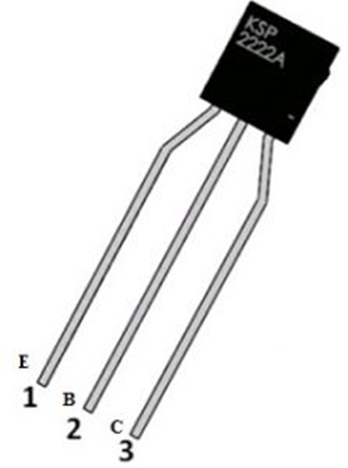
Collector and emitter terminals are open, and no current flows through the transistor while its base terminal is grounded, a condition known as reverse bias. When the transistor’s base terminal is linked to the power source, the transistor is forward-biased (closed), allowing current to flow between the collector and emitter terminals.
The specifications for the KSP2222A transistor are as follows:
● This transistor has a To-92 package type and is a bi-polar NPN high current transistor.
● DC gain (hFE) has a range of 100 to 300.
● The Emitter-to-Base Voltage (VBE) limit is 6 Volts.
● The collector current (IC) is capped at 600 milliamps (continuous)
● 40 Volts is the greatest Collector-to-Emitter Voltage (VCE) possible.
● Five milliAmps is the highest Base Current IB allowed.
● 75 Volts is the highest possible Collector-to-Base voltage.
● At the collector terminal, 0.625 Watts of electricity are dissipated overall.
● The highest noise level is 4 dB.
● Maximum 300 MHz is the transition frequency range.
● The working and storage junction temperatures range from -55°C to +150°C.
The KSP2222A is a 2N2222A direct replacement and is also an NPN bipolar general-purpose transistor with many uses. Collector current Ic and Collector-to-emitter voltage VBE are the only two distinguishing characteristics of the two NPN transistors. This transistor functions as an amplifier and a switch in most applications.
Each transistor’s primary and default role is that of a Switch. It functions similarly to a mechanical switch but is operated by electrical signals instead of levers. The image below is a simplified version of the circuit used to turn a motor or load on and off using a KSP2222A NPN transistor.
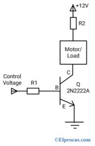
Here, the base current through the NPN transistor is restricted by base resistor R1. That way, transistors are protected. When the R2 resistor is wired into the motor’s ground, it regulates the amount of current that can travel into the collector.
When the voltage between the emitter and base terminals of the KSP2222A NPN transistor approaches and exceeds the threshold voltage, which is 6 Volts, the transistor begins conducting. When designing a circuit, it’s essential to choose the resistor carefully.
A transistor’s gain (HFE) is typically employed to magnify a current or voltage, making this application the most common one in which transistors are used. We can look at the schematic to further understand how the KSP2222A transistor fits into a common emitter (CE) amplifier. For voltage signals in the low-frequency region, the CE mode amplifier is the most used type of amplifier circuit (for example, audio signals).
Two resistors, R3 and R4, connect the supply voltage to the ground and the NPN transistor’s base and emitter pin, respectively, in the above circuit. The input voltage is connected to its base terminal to set the threshold voltage for the NPN transistor. A potential divider is created by connecting R6 and R4. Capacitors C1 and C2 are utilized to create a filter.
The circuit’s capacitor and resistor settings are presumed to be appropriate for the assumed application and NPN transistor. The primary drawback of this amplifier circuit is that it cannot handle voltage signals at very high frequencies. Op-amps (a collection of transistors in a single package) is utilized for fast and simple amplification in such situations.
We hope that this article has been helpful to you. We have more interesting articles on our website that could benefit you, just like this one, so feel free to browse through our website to learn more.
Please contact ICRFQ if you have any more questions or would like to place an order for a KSP2222A transistor. In China, we are the top choice for electronic component distribution.
WhatsApp us