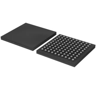
LPC1768FET100
Part Number: LPC1768FET100
Manufacturer: NXP Semiconductors
Description: ARM Microcontrollers – MCU 512K FL ETHERNET USB LQFP100
Shipped from: Shenzhen/HK Warehouse
Stock Available: Check with us
ICRFQ.com - Electronic Components Distributor in China Since 2003

Part Number: LPC1768FET100
Manufacturer: NXP Semiconductors
Description: ARM Microcontrollers – MCU 512K FL ETHERNET USB LQFP100
Shipped from: Shenzhen/HK Warehouse
Stock Available: Check with us
| Category | Integrated Circuits (ICs) |
|---|---|
| Family | Embedded – Microcontrollers |
| Manufacturer | NXP Semiconductors |
| Series | LPC17xx |
| Packaging | Tray |
| Part Status | Active |
| Core Processor | ARM? Cortex?-M3 |
| Core Size | 32-Bit |
| Speed | 100MHz |
| Connectivity | CAN, Ethernet, I2C, IrDA, Microwire, SPI, SSI, UART/USART, USB OTG |
| Peripherals | Brown-out Detect/Reset, DMA, I2S, Motor Control PWM, POR, PWM, WDT |
| Number of I/O | 70 |
| Program Memory Size | 512KB (512K x 8) |
| Program Memory Type | FLASH |
| EEPROM Size | – |
| RAM Size | 64K x 8 |
| Voltage – Supply (Vcc/Vdd) | 2.4 V ~ 3.6 V |
| Data Converters | A/D 8x12b, D/A 1x10b |
| Oscillator Type | Internal |
| Operating Temperature | -40°C ~ 85°C (TA) |
| Package / Case | 100-TFBGA |
| Supplier Device Package | 100-TFBGA (9×9) |
The LPC1769, LPC1768, LPC1767, LPC1766, LPC1765, and LPC1763, all based on the ARM Cortex-M3, are highly integrated, low-power microcontrollers designed for embedded applications. The Arm Cortex-M3 is a next-generation core with improved system features like streamlined debugging and tighter integration of support blocks. Up to 100 MHz of CPU speed is available on the LPC1768/67/66/65/64/63. The maximum CPU frequency supported by the LPC1769 is 120 MHz. The Arm Cortex-M3 central processing unit (CPU) has a three-stage pipeline based on the Harvard design, which features local instruction and data buses and a third bus for peripherals. In addition to its speculative branching capabilities, the Arm Cortex-M3 CPU features an internal prefetch unit.
On-chip SRAM includes:
Arm’s Cortex-M3 microprocessor is a 32-bit, general-purpose chip with impressive speed and low power consumption. The Arm Cortex-M3 has a Thumb-2 instruction set, soft interrupt latency, hardware divide, interruptible/continuous multiple load and store instructions, automatic state save and restore for interrupts, a tightly integrated interrupt controller with a wake-up interrupt controller, and numerous core buses. In order to ensure that the processing and memory systems can function continuously, pipeline techniques are used. In the time it takes to execute a single instruction, two others will have been fetched from memory and decoded.
The LPC17xx has on-chip flash memory with a maximum capacity of 512 kilobytes. A new two-port flash accelerator has been developed to get the most out of the two lightning-fast AHB-Lite buses.
The LPC17xx has 64 kilobytes of static RAM on the chip. Two additional SRAM blocks of 16 kB each are located on a dedicated slave port on the AHB multilayer matrix, in addition to the leading 32 kB SRAM that can be accessed by the CPU and DMA controller via a faster bus. This design makes all three RAMs available simultaneously to the CPU and DMA, which greatly improves performance.
Memory Protection Units (MPUs) like the one found on the LPC17xx can lock down sensitive information within a user’s program, making for a more trustworthy embedded system.
By preventing processes from accessing one another’s data, blocking access to memory regions, defining memory regions as read-only, and detecting random memory accesses that could cause system failure, the MPU makes it possible to partition processing tasks. The memory protection unit (MPU) partitions memory into secure areas and blocks unauthorized access to specific areas. The MPU supports a maximum of 8 regions and 8 subregions per region. If an attempt is made to access a memory address that is not part of the MPU regions or is not allowed by the region setting, the Memory Management Fault exception will be thrown.
There is only one interrupt line from each peripheral device to the NVIC, but each device may have multiple interrupt flags. A single interrupt flag can represent various interrupt sources. A rising edge, falling edge, or both can be programmed to trigger an interrupt on any 42 pins available across Port 0 and Port 2 (the two ports).
You can assign multiple purposes to individual pins using the microcontroller’s pin connect block. Configuration registers operate the multiplexers that mediate communication between the pin and the on-chip peripherals. Before turning on a peripheral and enabling any associated interrupts, ensure it is connected to the correct pins. Any enabled peripheral function without a corresponding pin should be treated as if it were not doing anything. Open-drain outputs, pull-up, pull-down, and no resistor settings are available for most pins.
The LPC1768FET100,551 is a highly integrated, low-power-consumption, 100MHz Cortex-M3 microcontroller unit with 512kB flash, 64kB SRAM, Ethernet, and USB for embedded applications. It has a media access controller (MAC) for Ethernet, a USB device, an 8-channel DMA controller, an interface for quadrature encoders, a PWM with six outputs, an ultra-low power real-time clock with a battery backup, and up to seventy I/O pins for other uses.
Contact ICRFQ, your one-stop shop for purchasing electronic components in China, if you need further information or wish to place an order for the LPC2368FBD100. We will work hard to ensure you get the best possible products at affordable prices.
WhatsApp us