
Last Updated on October 22, 2023 by Kevin Chen
Printed circuit boards are used in all electronics and gadgets we use daily. A single layer or multiple layers can be used to create PCBs. The many layers, the design, and prospective applications must be the subject of many questions for you as a PCB designer. We have written this comprehensive reference on PCB layers to address all your PCB inquiries and layers.
What are PCB Layers
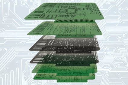
All the electrical equipment you see around you is made of printed circuit boards or PCBs. A single layer or numerous layers of conductive copper foils are used to create a printed circuit board (PCB).
A single PCB is created by stacking multiple double-layer PCB layers. PCB layers refer to the various circuit board layers. Heat-resistant insulation is sandwiched between the PCB layers and used to glue them together. A dielectric solder mask is used to seal the outer layers.
Layer Stack up
Before the layout design, a PCB is created by a process known as stack-up, in which copper and insulating layers are arranged. With a layer stack-up, you can fit more circuitry on one board.
Crosstalk, outside noise, and radiation can all be reduced thanks to the stack-up. With the right PCB stack-up, you can achieve excellent signal integrity while enhancing the device’s electromagnetic compatibility.
Multilevel printed circuit boards always benefit from stacked PCB configurations.
The positioning of the PCB layers is known as layer stack-up. A PCB is made up of conductive copper foil layers called PCB layers.
PCB Layers Type
The number of layers a PCB should have depended on its use and purpose. We’ll examine the most typical PCB layer types in this chapter.
Layer PCB
Since the 1950s, one-layer PCBs, sometimes known as single-layer PCBs, have been in use. It is still frequently utilized in everyday household appliances throughout the world. A dielectric material, one laminated conductive layer, and one soldered layer of material make up the one-layer PCB.
Due to their simple design and affordable production costs, single-layer PCBs are easily produced in bulk. There are fewer odds of any production issues because of how straightforward the system is. Due to the producers’ ease in understanding the construction, you may buy a lot of components quickly.
Many straightforward office and home appliances, such as the cheap calculators and alarm clocks you can buy at the shop, use one-layer PCBs. They are also found in kitchen appliances like coffee makers. They are occasionally used in surveillance cameras, LED lights, and printers.
A single thermally conductive dielectric is installed on the single-layer PCB, followed by a copper laminate and a solder mask. Typically, copper laminate is used to create PCBs, ranging in thickness from one to twenty ounces.
The operating temperature range for one-layer PCBs is between 130 and 230 degrees C.
Two Layers PCB
The next technical advancement following a single-layer PCB is a double-layer PCB. Due to its greater capacity, it is the most widely used form of PCB worldwide. They are more widely utilized in electronic products and easier to build than the various multi-layer PCBs today.
The double-layer PCB has numerous advantages. Because the bottom and topsides match, it has higher routing traces. Due to its adaptability, it can be used for various purposes. Its high density and cheap manufacturing cost make it suitable for usage in contemporary appliances and gadgets. Different firms’ residential HVAC systems use double-layered PCBs.
A large variety of computer printers and music industry amplifiers both employ two-layer PCBs.
Inverted mirror representation is present at the bottom of the double-layer PCB, which resembles the one-layer PCB elsewhere. In a two-layer PCB, the dielectric layer is likewise thicker and is laminated with copper on the bottom and top sides. The copper is then on both sides, covered with a solder mask.
Four Layers PCB
The latter has a more complex design comparing four layers of PCB to single and double-layered PCB. It has many rows, unlike single or double-layered PCBs, which only have one row of dielectric material. The bottom and top solder masks are separated by numerous layers of copper and other conductive material, much like any multilevel PCB.
Durability and being more effective than single- and double-layered PCBs are two advantages of 4 layers PC. It is also compact and suitable for various electronic gadgets. The component’s adaptability makes it appropriate for both straightforward and complex tools.
Additionally secure, it avoids electromagnetic interference. Due to its less weight, you can also utilize it in advanced systems.
Four layers of PCB are used in several handheld gadgets, such as tablets and smartphones. They can also be found in planet-orbiting satellite systems. They are also utilized in the equipment for in-depth space exploration space probes.
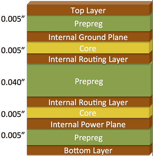
The four-layer PCB comprises three inner dielectric layers with one core, two prepreg layers, and four conductive copper layers. The bottom and top are then covered with dual dielectric solder mask layers.
Six Layers PCB
A wide range of electrical gadgets, commercial applications, and technological equipment are powered by six PCB layers, which are part of modern multi-layer PCBs.
Those with six layers are more robust and thicker than double- or four-layer PCBs. Along with being more technologically advanced, it is also small. They are capable and reducing the possibility of crosstalk and electromagnetic interference because they have six layers.
On desktop and laptop computers, you’ll find six PCB layers used in advanced computing applications. They are even present in hard disks employed as data storage. Fire alarm systems are made more effective by the PCBs, which are also used in such systems.
Moreover, six layers of PCBs can be seen in industrial controlling systems, fiber optic receivers, GPS devices, industrial controlling systems, mobile phone transmission, and medical equipment like heart monitors.
The six-layer PCB structure is comparable to the four-layer PCB, but it has two more rows of copper and two additional layers of dielectric material. The cores are located in the arrangement’s second and fourth rows of dielectric material. The second and fifth rows of conductive copper are called “planes,” while the other three are “signals.”
Eight Layers PCB
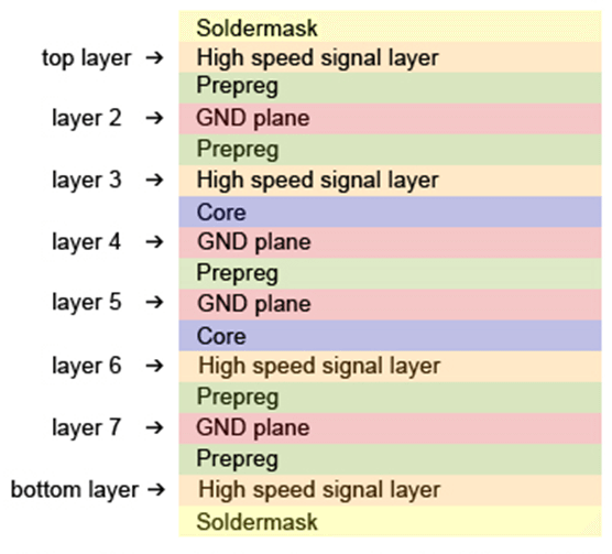
PCBs with eight layers are fantastic tools for maximizing electronic gadgets’ effectiveness and computing capability. Although it has four copper signal layers and four plane layers, the eight-layer PCB is very similar to the six-layer PCB.
The eight layers of PCB are used in several computer systems and high-tech gadgets. Our ability to go from kHz computer frequencies to the GHz high-speed gadgets of the present day is due to their invention.
Eight PCB layers are used in various governmental, aerospace, healthcare, and commercial applications.
This PCB consists of seven rows of inner dielectric material, which hold the eight layers together. The eight PCB layers on the top and bottom components are sealed with a dielectric solder mask. The eight layers PCB and the six layers PCB share a lot of similarities, although the latter has extra pairs of prepreg and copper columns.
What Is A Multi-layer PCB?
One layer of conductive material makes up a single layer PCB. On one side of the board is a mounted conductive wiring pattern, and on the other, there are components. Since no wires can cross for a good circuit to function, single-layer PCBs are frequently employed in straightforward electronics. Like a single-sided PCB, a double-sided PCB has more layers than a single-sided board but less than a multi-layer PCB. They have a single dielectric layer and a conductive metal layer on either side.
Contrarily, multi-layer boards are more complicated than single-layer or double-sided PCBs. Three or more conductive layers are present on a multi-layer PCB. On top of this core, more layers—often copper foil—stack.
One of the top manufacturers of multi-layer PCBs is Millennium Circuits. Starting with the core, we are aware of how things are made. After then, the subsequent layers are not entirely healed. This is necessary for the manufacturer to adjust them with respect to the core. Then, through a lamination process, foil is applied and might alternate with other layers. It is crucial to join the layers and securely melt them together using high-pressure and temperature methods.
Single Layer vs Multilayer PCBs
Multilayer PCBs have a lot of advantages. These boards are lighter and smaller overall, making them ideal for cellphones, PCs, or any other device that requires adaptability packed into a compact design. Here are a few particular advantages:
- The multiple layers of multi-layer PCBs allow for a higher level of functionality.
- The building is simpler when there is no need for connectors for numerous distinct PCBs.
- You will receive a high-quality, productive product thanks to strict testing procedures used during the manufacturing stage.
- Greater speed than a single-layer board is possible thanks to the electrical qualities of multi-layer PCBs.
- Multilayer PCBs can be useful for robust and flexible construction, based on how many layers you decide to add.
The drawbacks of single-layer PCBs, on the other hand, should not be disregarded even though they are quite beneficial in particular applications. A few drawbacks of single-layer boards are as follows:
● Single-layer boards don’t give as much diversity in their use because wires cannot cross them, making them best suited for basic electronic devices.
● Single-layer PCBs are less expensive to produce but less durable than multi-layer ones, making them less cost-effective overall.
● PCBs with a single layer can’t operate at the same high speeds as those with multiple layers.
● Because there is just one side conductor on single-layer boards and every line needs its channel, this limits the circuit design options.
● While single-layer PCBs can be used for low-density designs, multi-layer PCBs are the ideal alternative for many sectors looking for a more robust and adaptable solution.
Multilayer vs Double-sided Layer PCBs
In a double-sided (or double-layer) PCB, a metal layer is present on both sides of the material (or substrate). They are frequently found in various consumer electronics, including phones and other gadgets like power monitors, test equipment, and amplifiers.
Function and schematic requirements determine whether you need single-sided or multi-layer PCBs. Making a schematic, which describes the electrical design of the purpose and function of the board, is one of the initial phases in the PCB layout procedure. The chief engineer will decide throughout the schematic development if the materials and components can function within a double-side layer or whether further layers are required.
Why do we need multi-layer PCB?
In the last few decades, electronics have advanced quickly. In the 1990s, mobile phones could only be used to make calls or receive messages. Still, today we have practically built an entire computer into these little portable devices, and we couldn’t have done it without Multilayer PCBs. Electronic products become smarter by being smaller and more portable thanks to multi-layer PCB and SMD components.
The current world is moving toward downsizing, and multi-layer PCB is serving as the foundation. Since multi-layer PCB is designed in PCB industries using cutting-edge PCB machines, it complies with all regulations and is more durable than simple PCB boards. Multilayer PCB design plays a significant role in defining the functional and thermal performance of the entire electronic system. Multilayer PCB is used in advanced electronic goods because it enables the incorporation of many components on a single board, resulting in a higher component density.
Are multi-layer PCBs better than double-sided ones?
The use that will be made of the finished board will determine the answer. Although producing multi-layer designs costs more, there are many situations when they are advantageous or necessary. They frequently enable more sophisticated circuits in a smaller footprint, which is why this happens. Key benefits of multi-layer PCBs could be:
- Enhanced durability – Stacking additional layers together achieves a more robust physical design.
- Overall quality – because they are intrinsically more difficult to construct and design, the manufacturing process is frequently more exacting.
- Better for more complicated or powerful circuit designs, some performance devices’ speed and capacity needs may necessitate a multilayered PCB design.
- Space-saving: By stacking conductive layers, the footprint can be lowered, allowing larger circuits to fit on a smaller, lighter board.
- Multiple independent PCBs would need to be powered separately; a multi-layer design often only needs one such input. Single connection point
Conclusion
PCBs power many societal devices and industries. Different kinds of PCBs are becoming increasingly necessary as our technology advances. The possibilities may appear too numerous as you decide between a single and multi-layer PCB. Before you spend money on a new PCB, it’s critical to comprehend the advantages and disadvantages of each choice.
For more detail on designing, manufacturing or purchase of multilayer PCBs, contact us at ICRFQ. We manufacture the best electrical components in China.
If you want to find more Electronic Components Distributors, please check out the following articles:
Electronic Components Distributors In the USA
Electronic Components Distributors In UK
Electronic Components Distributors In China
Electronic Components Distributors In India
Electronic Components Distributors In Singapore
Electronic Components Distributors In Malaysia
Electronic Components Distributors In Vietnam
Electronic Components Distributors In South Korea
- Where to buy IC chips? The Best Guide? - March 26, 2024
- Breaking Down Barriers: Overcoming Obstacles in Cross-Border Electronic Component Trade - March 4, 2024
- Everything You Need to Know About Amplifier IC Chips - March 4, 2024


