
Last Updated on October 22, 2023 by Kevin Chen
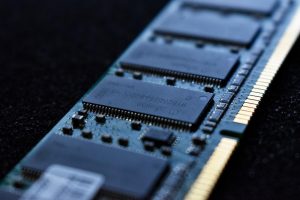
Image Source: Unsplash
NAND flash memory is fast becoming one of the most widely used non-volatile storage components in electronics, ranging from mobile devices to data centers.
With its superior read and write performance and durable storage capacity, NAND flash IC continues to break new grounds in the world of electronics.
If you are exploring opportunities to use NAND flash technology in your next embedded system design, this blog post will help you understand what it is, its different types, and its common applications in electronic systems.
Moreover, we’ve also listed a few important considerations when buying an NAND flash memory chip for your next project, including how to choose the best NAND flash IC distributor in China
What is NAND flash memory?
NAND flash is a type of non-volatile electronic storage that does not require any form of power to store and retain data. It is a type of flash memory that uses a floating gate to store data.
NAND flash is different from NOR flash in that it uses a single transistor to store each bit of data, while NOR flash uses multiple transistors per bit. It is also much slower than NOR flash but can be produced with higher storage density and at a lower cost.
NAND flash memory has become the most widely used non-volatile storage component in electronics due to its fast write and read performance, high storage capacity, and low cost.
It is used for applications such as solid-state drives (SSDs), USB drives, SD cards, digital cameras, portable music players, and smartphones.
Data in the NAND flash IC is saved in the form of electric blocks. The saving process is made possible by an electric circuit.
History of NAND flash
NAND flash traces its roots to the development of metal-oxide-semiconductor field-effect transistors(MOSFET) in the late 1950s.
The development was hastened by the invention of the floating gate MOSFET in 1967.
During the MOSFET development phase, engineers realized that it was possible for these gates to hold their states without an external power source.
This discovery led to the invention of EEPROM in 1972, which was the first non-volatile memory.
NAND flash was invented by Fujio Masuoka while working for Toshiba in 1984.
The name NAND flash comes from the structure of the device, which consists of a series of floating-gate transistors connected in a “NAND” configuration.
In 1988, the world’s first NAND-type flash chip was created by Toshiba and SanDisk. In 1999, SanDisk developed its first solid state drive using NAND flash memory which it called the Secure Digital (SD) card. In 2000, Samsung Electronics introduced its first NAND flash drive under the name Samsung Mobile Module which was capable of storing 256 MB of data. In 2004, Samsung Electronics introduced its first 2 GB SD card using single-level cell (SLC) technology and later went on to develop multi-level cell (MLC) technology.
The following year saw advancements made by other companies such as Lexar and Kingston Technology Company who developed their own 2 GB SD cards using MLC technology.
The next year saw further advances as companies like Patriot Memory introduced thumb drives with 4 GB storage capacity and Verbatim Corporation introduced 8 GB USB drives with MLC technology.
Since then, different manufacturers have been making great strides when it comes to designing and developing NAND flash IC. This has also increased the usability and applications of these chips.
The market has also grown big and you can now buy the NAND flash IC easily from a reputable distributor in China.
NAND flash IC in operation-how it works
To understand how a NAND flash IC works, it is important to first understand the basic electrical operation of a transistor.
A transistor can be used as a switch that is controlled by a voltage applied to its control terminal.
One transistor is known as the floating gate while the other one is known as the control gate.
The primary purpose of the control gate is to connect the floating gate to its ideal position in the grid.
Now, let’s discuss the operation of the NAND flash memory.
The NAND flash memory is made of a number of memory cells.
Each cell has one transistor and a single floating gate.
The number of cells in the array depends on the size and capacity of the NAND flash IC.
When you apply a voltage to the control gate, it attracts electrons to its surface.
These electrons are known as charge carriers or ions.
The control gate should have enough charge carriers to attract all the electrons on the floating gate.
These electrons are attracted to the surface of the floating gate, thereby rendering it negative in electrical charge.
This creates a field around each bit that attracts negative charges and repels positive charges.
This is what makes it possible for us to record data in NAND flash IC components by applying voltage pulses during operation.
The result is stored as binary data in each cell and can be read by measuring how much charge was removed from each cell by applying specific voltages during operation. This set of operations is also known as the Program-erase-read cycle or P-E-R cycle for short.
This whole process of charging and tunneling happens in the flash cell can have negative effects on the transistors. To avoid this, there is a fixed number in which the cells can be programmed and erased.
Types of NAND flash IC
There are several types of NAND flash memory available in the market today. The most common types are listed below:
SLC (Single Level Cell)
SLC stores one bit of data per cell using two levels (0 or 1). Theoretically, an SLC can store up to twice the capacity as an MLC chip because it only requires half the number of bits per cell. However, since an SLC has only two levels per cell (as opposed to four levels for MLC), it can only store half as much information as an MLC chip before errors occur. Therefore, SLCs tend to be more expensive than MLC chips because they use more raw materials. Furthermore, they tend to have slower read and write times.
MLC (Multi Level Cell)
MLC stores two bits of data per cell using four levels (00, 01, 10, 11).
Compared to the SLC, it has lesser endurance. This makes it a cheaper option for you.
Most PCs in the market run on the MLC.
QLC(Quad Level Cell)
QLC stores four bits of data per cell using eight levels (000, 001, 010, 011, 100, 101, 110 and 111).
QLC is currently in the development stages.
But is generally cheaper than the top two options.
Toggle Flash
Toggle flash memory is a type of non-volatile NAND flash memory developed by Intel Corporation.
It uses a process similar to NOR flash memory but it has a faster write speed than NOR flash.
It also has the ability to read from either side of the chip. It does not have any bad blocks and can be used as a drop-in replacement for NOR flash memory.
3D NAND
3D NAND is another type of non-volatile NAND flash memory developed by Intel Corporation and Toshiba. This new technology stacks floating gate transistors on top of each other to increase storage density.
The main advantage of this technology over other types of NAND is that it can be scaled without degrading performance since it requires the same number of processing steps no matter what capacity is being made; unlike multi-level cells (MLC), which need extra processing steps for each added level or single-level cells (SLC), which have limited life spans when programmed too many times.
Reasons why is NAND flash ICs are so popular?
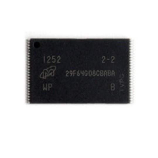
Image source Olifex
NAND flash is so popular because it has a number of benefits that make it a better choice for many applications. These include:
– Economical cost: One of the primary reasons why NAND flash is so popular is because it is a very economical storage option. Compared to other non-volatile storage options like magnetic disks, NAND flash is much cheaper. Also, NAND flash requires much less power to operate, which results in lower operational costs.
– High storage capacity: Another reason why NAND flash is so widely used is its high storage capacity. Depending on the technology used and the number of layers in the chip, NAND flash chips have been able to store up to hundreds of gigabytes of data.
– High performance: Most NAND flash chips can read and write data at a very high speed. This is because they use a type of non-volatile memory called ‘flash memory. Unlike hard disk drives, which use mechanical arms to read and write data, flash memory uses transistors. They are much faster than mechanical arms because they do not need to move in order to access the data.
– Low power consumption: As mentioned above, NAND flash chips use less power than hard disk drives and other storage devices. This makes them ideal for applications where power is a concern.
– Low latency: In terms of latency (the time it takes for a device to respond), NAND flash ranks among the lowest compared to other storage devices such as hard disk drives.
Limitations of NAND flash IC
NAND flash is an amazing storage device, but it does have a few limitations that system designers need to be aware of. These include: –
-Fixed number of P/E cycles: A typical flash memory has finite number of program/erase cycles before it fails. After that, the memory cannot be erased or programmed again.
-Limited write endurance: NAND flash can only endure a certain number of erase/programming cycles before it is no longer able to work. This is a major limitation for applications such as embedded systems where the device may need to be reprogrammed frequently.
-Vulnerable to high energy particles: Potent energy particles such as X-rays can distort data on the NAND flash memory devices. They can easily change the 0s and 1s into unreadable data.
Technical specs of NAND flash IC
Before you buy a NAND flash chip, it is important that you pay attention to its technical specifications.
These specs include:
-Memory capacity: The memory capacity of a NAND flash chip is measured in megabytes (MB) or gigabytes (GB).
-Package type: The package type refers to the physical shape and size of the NAND flash memory IC. Common package types include 8-pin SOIC, 8-pin PDIP, 16-pin SOIC, 20-pin SOIC, 24-pin QSOP, 28-pin SSOP and 32-pin TSOP.
-Programming voltage: The programming voltage of a NAND flash chip is the minimum voltage needed to store data on the device.
-Read voltage: The read voltage of a NAND flash chip is the minimum voltage needed to retrieve data from the device.
-Programming time: The programming time refers to the amount of time needed for programming a NAND flash memory IC.
-Erase time: The erase time refers to the amount of time needed for erasing a NAND flash memory IC.
-Data retention: Data retention is measured in terms of years. It indicates how long your data can be retained without being lost because of power failure, etc. If a memory chip has a data retention rate of 10 years, it means that your data can survive up to 10 years without power.
-Data remanence: Data remanence refers to how much magnetic field would be required to overwrite your old data on a memory chip. If it has high remanence, you need stronger magnetic fields to overwrite your old data with newer ones.
Conclusion
At the end of it all, ensure that you choose a reputable NAND flash IC distributor in China that has a good reputation.
This is the surest way of ensuring that you end up with a perfect flash memory chip.
Check out the reviews of the Flash Memory IC distributors you are considering.
You can also check out the feedback of the customers who have bought from them.
This will help you to make an informed decision about the NAND flash IC distributor that you should trust.
In today’s world, it is not always easy to get into contact with a NAND flash IC distributor in China directly, but with this guide, you should be able to reach out to us at ICRFQ.
We will source your IC from the best distributor in China at reasonable price.
If you want to find more Electronic Components Distributors, please check out the following articles:
Electronic Components Distributors In the USA
Electronic Components Distributors In UK
Electronic Components Distributors In China
Electronic Components Distributors In India
Electronic Components Distributors In Singapore
Electronic Components Distributors In Malaysia
Electronic Components Distributors In Vietnam
Electronic Components Distributors In South Korea
- Where to buy IC chips? The Best Guide? - March 26, 2024
- Breaking Down Barriers: Overcoming Obstacles in Cross-Border Electronic Component Trade - March 4, 2024
- Everything You Need to Know About Amplifier IC Chips - March 4, 2024


