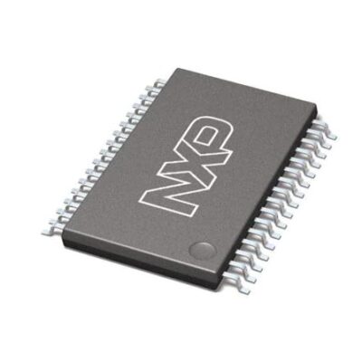
PCA9622DR
Part Number: PCA9622DR
Manufacturer: NXP USA Inc
Description: IC LED DRV LIN PWM 100MA 32TSSOP
Shipped from: Shenzhen/HK Warehouse
Stock Available: Check with us
ICRFQ.com - Electronic Components Distributor in China Since 2003

Part Number: PCA9622DR
Manufacturer: NXP USA Inc
Description: IC LED DRV LIN PWM 100MA 32TSSOP
Shipped from: Shenzhen/HK Warehouse
Stock Available: Check with us
| Datasheet | |
|---|---|
| Category | Integrated Circuits (ICs) |
| Family | PMIC – LED Drivers |
| Manufacturer | NXP Semiconductors |
| Series | – |
| Packaging | Tape & Reel (TR) |
| Part Status | Active |
| Type | Linear |
| Topology | – |
| Internal Switch(s) | Yes |
| Number of Outputs | 16 |
| Voltage – Supply (Min) | 2.3V |
| Voltage – Supply (Max) | 5.5V |
| Voltage – Output | 40V |
| Current – Output / Channel | 100mA |
| Frequency | 100kHz ~ 1MHz |
| Dimming | PWM |
| Applications | Backlight |
| Operating Temperature | -40°C ~ 85°C (TA) |
| Mounting Type | Surface Mount |
| Package / Case | 32-TSSOP (0.240″, 6.10mm Width) |
| Supplier Device Package | 32-TSSOP |
The PCA9622 is a 16-bit LED driver controlled by an I2C bus, ideal for flashing and dimming 100 mA Red, Green, Blue, and Amber (RGBA) LEDs with a voltage switch. Each LED output is controlled by its independent PWM circuit with a constant frequency of 97 kHz and a duty cycle that can be adjusted from 0% to 99.6%. A group PWM controller with 8 bits of resolution (256 steps) may dim or flash all LEDs at the same value. The constant frequency is 190 Hz, and the adjustable frequency ranges from 24 Hz to once every 10.73 seconds, with the duty cycle ranging from 0% to 99.6%.
Every LED output can be turned off or on (with no PWM control), changed to a custom value using the PWM controller, or set to the same custom value as the other outputs in the group. The input voltage range for the PCA9622 is 2.3 V to 5.5 V, while the maximum output voltage for the 100 mA open-drain outputs is 40 V. The PCA9622 is a pioneering member of the Fast-mode Plus (Fm+) family of LED controllers. More people can use the bus at once because of the increased frequency (up to 1 MHz) offered by Fm+ devices (up to 4000 pF). When several devices need to be dimmed or blinked simultaneously without software control, the active LOW Output Enable input pin (OE) causes all the LED outputs to flicker and can be used externally to PWM the outputs.
All or defined groups of PCA9622 devices can respond to a shared I2C-bus address, allowing, for example, all red LEDs to be switched on or off simultaneously or marquee chasing effect, minimizing I2C-bus commands. This is accomplished using a software-programmable LED Group and three Sub Call I2C-bus addresses. For maximum compatibility, a total of 126 devices can share a single bus using only seven hardware address pins. In the same way as the Power-On Reset (POR) initializes the registers to their default state, setting the outputs to HIGH, the Software Reset (SWRST) Call allows the master to do a reset of the PCA9622 via the I2C-bus (LED off).
This facilitates a rapid and painless method of setting all device registers to the same state. If the current or voltage provided by the PCA9622’s on-chip 100 mA NAND FETs is insufficient to drive the LEDs, the PCA9635 with a bigger current or higher voltage external drivers can be used instead. The software for PCA9622, PCA9625, and PCA9635 is interchangeable.
Off
On
Programmable LED brightness
IDs Bus masters must output slave addresses after START. Seven hardware address pins allow 128 programmable addresses. Because Software Reset and LED All Call are ON by default, only 126 addresses can be used. Other reserved addresses and Sub Call addresses decrease the number of viable addresses.
Remark: When internal global blinking is selected (DMBLNK = 1, MODE2 register), OE as an external control signal produces an indeterminate blinking pattern. OE as an external dimming control signal when internal global dimming is selected (DMBLNK = 0, MODE2 register), has an indeterminate dimming pattern.
The PCA9622 stays reset until VDD reaches VPOR when power is provided. After releasing the reset condition, the PCA9622 registers and I2C-bus state machine are initialized to their default states (all zeroes), deselecting all channels. To reset the device, VDD must drop to 0.2 V.
The Software Reset Call (SWRST Call) resets all I2C-bus devices to power-up status using a specific formatted command. It requires a working I2C bus and no devices on it.
The transmitter-to-receiver data flow between START and STOP is unlimited. Each 8-bit byte is acknowledged. The transmitter sets the bus to HIGH while the master generates an acknowledge-related clock pulse. Slave receivers must acknowledge each byte.
Also, a master must generate an acknowledgment after the reception of each byte clocked out of the slave transmitter. The device that acknowledges has to pull down the SDA line during the accept clock pulse so that the SDA line is stable LOW during the HIGH period of the acknowledge-related clock pulse; set-up time and hold time must be taken into account. A master receiver must signal an end of data to the transmitter by not generating an acknowledgment on the last byte clocked out of the enslaved person. In this event, the transmitter must leave the data line HIGH to enable the master to generate a STOP condition.
Contact ICRFQ, your one-stop shop for purchasing electronic components in China, if you need further information or wish to place an order for the PCA9622DR. We will work hard to ensure you get the best possible products at affordable prices.
WhatsApp us