
Last Updated on April 10, 2022 by Kevin Chen
PCB assembly is a complex and crucial process in the Electronics Industry. It involves the process of assembling a printed circuit board or an electronic circuit with the help of semiconductors and other electronic components. The PCB assembly process is a combination of many processes that work towards the final goal of manufacturing the finished printed circuit board.
Let’s explore the ins and outs of the PCB assembly process from the various components used, the equipment required, to the various steps involved.
PCB Terminologies
To understand the PCB assembly process, it will be good to go through some of the most common phrases that are used during the process. They include:
-Substrate: A PCB substrate is a base on which the printed circuit board is built. The most commonly used substrate material is fiberglass epoxy laminate.
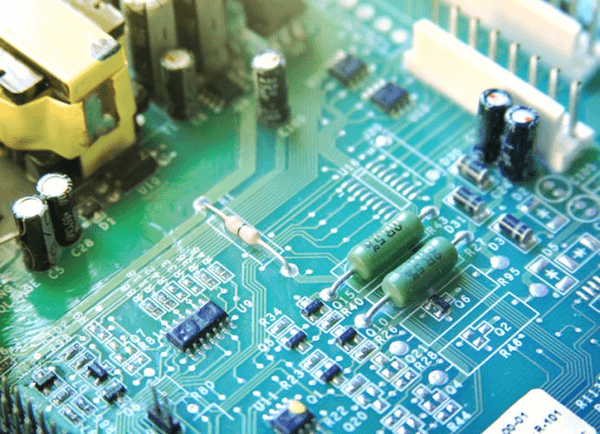
-Circuit Board: A circuit board is an electronic component that is used to manufacture various electronic devices. It can be made up of a single or multiple layers, where the layer number depends on the complexity of the device being manufactured. The circuit board provides a platform for all electronic components to be mounted onto it and allows them to communicate with each other through connectors or conductive pathways.
-Routing: Routing refers to the process of connecting different components and making them functional, by using a track on a PCB.
-Drilling: Drilling refers to the process of creating holes in printed circuit boards for mounting components such as capacitors and resistors, etc. These holes are created by drilling machines that are specifically designed for this purpose and are also referred to as drill presses or drilling machines in PCB assembly processes.
-Copper: Each active side of a PCB comprises copper layers. The primary role of copper is to play the conductive role, ie, to facilitate the flow of current in the PCB. If the PCB is double-sided, that is if both sides are active, then you should expect to see the copper layers on both sides.
-Solder mask: A solder mask is a thin layer of a protective coating that is applied over the surface of the PCB after the copper has been etched. The solder mask provides a physical barrier to prevent solder from flowing onto unwanted areas and also protects the copper from oxidation.
-Silkscreen: Silkscreen refers to a layer of ink that is applied over the surface of the solder mask and printed with text or graphics. It serves as an aid for assembly and maintenance personnel, who can easily read information like part numbers, component orientation, etc., printed on it.
-Drill holes: The drill holes are used to mount components onto PCBs. These holes are created by drilling machines that are specifically designed for this purpose and are also referred to as drill presses or drilling machines in PCB assembly processes.
-Holes: Holes refer to any open area in a circuit board that does not contain any conductive traces or components mounted on it. Holes can be created by etching the copper on the board or by drilling machines.
-Circuit traces: Circuit traces are the conductive traces that conduct signals from one component to another. They are created by filling a circuit board with a thick, conductive paste and then etching away the unwanted areas of the PCB.
-Reflow: Reflow is a heating process used for soldering components on PCBs. Components on PCBs are mounted using solder paste, which is applied over the surface of the PCB in a thin layer and then reflowed using heat to attach components to the PCB.
-Flux: Flux is an acid or alkali substance that is used during soldering processes to clean unwanted oxides from metal surfaces and make them more receptive to solder.
-Pick and place machine: A pick and place machine picks up components from their bins and places them onto specific locations on PCBs automatically. This machine can also be used for placing resistors, and capacitors, among others.
-Manual soldering: Manual soldering is the process of manually applying solder to a PCB. This process is done by hand, but not by the human hand. It is done by machines that apply solder to PCBs to attach components manually.
-Wave soldering: Wave soldering is a process used to solder components on PCBs in which the PCBs are moved through a furnace that heats the PCB and components. The solder is melted by the heat of the furnace and flows over the components, attaching them to the PCB.
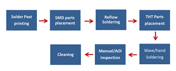
Summary of PCB assembly process
The process of creating a printed circuit board is broken down into different steps.
Step 1: Design
The first step in creating a printed circuit board is designing it. The designer first creates a layout of how they want their board to look and what they want it to do. This can be done with computers or by hand on a piece of paper. Designers then use software such as Cadence, and Allegro, among others, to create an electronic representation of their layout.
These programs allow designers to simulate connections between different elements such as resistors, capacitors, and ICs (Integrated Circuits). This allows designers to make sure that their design will work before they start making it on actual boards. Once designers have created their layout, they send it to a manufacturer for manufacturing.
Step 2: Layering
The second step of the PCB assembly process is the manufacturing of the board. Manufacturers first create a single layer (or “layer one”) of the board using a photolithography process.
The photolithography process involves exposing an acid-resistant coating on the board to light through a negative photomask. The acid-resistant coating protects the copper surface of the board during this process and allows only those areas exposed by the photomask to be etched away.
This etched area becomes the circuit traces of layer one. After etching away those areas, manufacturers then flood them with an etching solution that removes all of the exposed acid-resistant coating except for those traces.
When manufacturers have finished this process, they rinsed off all excess paste and dried the board.
Step 3: Solder mask
The third step in creating a PCB is adding the solder mask. This process involves using a photomask to expose the solder mask layer to light. The solder mask layer protects solder pads from being damaged during manufacturing and from being exposed to the elements after installation.
Once exposed, manufacturers flood the board with an etching solution that removes all of the exposed acid-resistant coating except for those areas that were masked by the photomask (solder pads). They then rinse off that etching solution and dry it.
Step 4: Quality control and inspection
Now that everything seems to be done the next step is to inspect and verify the quality of the PCB. This involves checking the solder mask, the circuit board, and the components.
The PCB is checked for any damage during production and any defects in the circuit design. The components are also verified to make sure that they fit correctly and that they are of high quality.
Step 5: Component fixation
In this step, the components are soldered onto the board. Any components that are not soldered in this step will be installed after the PCB has been completed.
The type and nature of components fixed on the PCB will always depend on the customer’s specifications and product requirements.
Step 6: Solder mask opening
This process involves removing any excess solder mask to expose small pads on the solder mask layer. This allows for a better connection between the component and the PCB and also helps with heat dissipation.
Some components are fixed on the holes that you had drilled in the previous steps. The dimensions of the holes should fit the components and guarantee their structural stability.
Step 7: Final inspection and testing
In this step, a final inspection is done to make sure that everything is working properly and that all of the components have been installed correctly.
The final testing involves making sure that all of the electrical connections work properly before shipping it off to customers.
Types of PCB Mounting Technologies
As we have mentioned, one of the steps in the PCB assembly process entails mounting the components on the surface. Different techniques and technologies are used in the mounting process.
Surface mounting technology (SMT)
This is one of the most common technologies for installing PCB components. It involves using pins and pads to connect the components to the board. The pins should be inserted into holes that have been drilled in the board before.
The surface mounting technology is usually used with surface mount components. These are small and low-power components that require mounting on a surface with a minimum number of connections. The SMT technology ensures that all of the electrical connections are made properly before it is sent to customers.
Steps for the surface mount technology
The basic steps for the SMT include:
The first step entails getting a solder tape template that will guide on how to install all the tiny components to their rightful positions on the PCB.
Before the components are placed, the stencil is inspected to ensure that the template is properly aligned. This minimizes any errors that could arise.
Now that the design and the template are ready, the board is passed forward to an automatic machine which places the components in their rightful places according to the designs.
These machines have reels that ensure all the components are aligned perfectly as desired.
Once the components are in place and meet the requirements a heating process is deployed. It solidifies the paste to ensure that the components remain glued to the surface.
Keep in mind that before the component placement, select areas of the PCB are coated with the solder paste. These areas or spots are chosen depending on the components that you would like to install. An adhesive may be added to enhance the stability of the components.
Through hole mounting technology (THT)
This technology involves inserting a pin through a hole in one side of the PCB, then connecting it to another pin on the opposite side of the board using solder paste or solder jointing paste.
THT is well-suited for thick boards, where more room is available for components in between them and where there are many places to fit pins or holes on both sides of the board at once.
Steps for the THT
First, the holes are drilled or punched on both sides of the PCB.
Then, the components are installed in their respective places by melting the paste and inserting them into their holes.
Finally, it is time to solder the pins.
The soldering process is done by applying solder to both sides of the board and then connecting them with a wire or a pin.
The result is a perfect connection between both sides of the board.
After that, it can be used as an ordinary circuit board.
Transistor mounting technology (TML)
This is a more complex method that involves using a specialized resin called an epoxy-based paste.
It comprises two components, one is liquid and the other component is powder. The liquid component acts as a glue, while the powder component acts as a filler.
The two components are mixed to form a paste that can be applied to the PCB using an applicator gun or by hand.
The paste is then heated to cure it.
After that, the paste is pressed using a special tool to create a nice flat surface for the component.
The result is a nice and solid connection between the component and the PCB.
Thin-film technology (TFT)
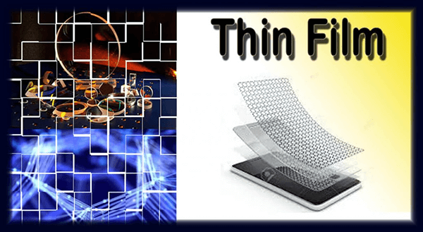
In this method, a thin film of copper or copper alloy is deposited on top of the PCB. This allows for higher conductivity and better heat dissipation in comparison to other technologies.
The advantages are that it allows for larger components to be used with less space between them as well as better heat dissipation.
However, this approach does not allow for components that have high power consumption due to the thinness of the film. It also has issues when soldering components because solder cannot be applied directly on top of it due to its thickness.
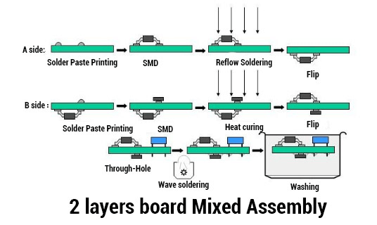
Mixed technology
This is among the most modern technologies used for mounting components on the PCB. The method encompasses numerous techniques that ensure both large and small components are perfectly embedded in the board.
Some of the techniques deployed in the mixed technology include;
-Single-sided mixed assembly: In this technique, both the SMT and THT techniques are used for mounting components on one side of the board.
-Split assembly: Here, the SMT and THT techniques are used for mounting components on both sides of the board.
-Double-sided mixed assembly: This is a combination of both the single-sided and split assembly techniques. This simply means that the SMT and SHT are deployed on both sides of the PCB.
The advantages of mixed technology are that it allows for high-density stacking of components on the PCB and allows for more space to be used between components.
This is because the thin film does not have to be as thick as other technologies, making it easier to solder components directly on top of it. The disadvantages are that solder cannot be applied directly onto the board due to its thinness, and also that soldering is more difficult than other technologies.
Mixed technology has been used by various companies as it seems to match the demand for the new products in the market. The technology is also suitable for complex electronic products whereby the use of one method only may not be sufficient.
Manual soldering vs Wave soldering: What is the difference?
As we have described, soldering is one of the methods in the PCB assembly process. Manual and wave are two methods of soldering. What is the difference between them?
As the name suggests, the manual is where a technician does the soldering by hand. It is generally used in small-scale applications and when there is a high level of precision.
Wave soldering is a process where the materials that are required to be used to solder are wrapped around a specialized rod, which is then heated up. It has been around for many years and it can be used in large-scale applications.
As we have seen, manual soldering has its advantages, but the major disadvantage is that it takes time to complete and it requires a lot of skill to do so. However, this method can be more efficient than wave soldering as it does not require much time and effort on the part of the technician.
Wave soldering also has its advantages as it does not require any skill and does not take much time at all. The technique is also more accurate since it eliminates any chances of human error during the soldering process.
Types of PCB inspection
We have also stated that inspection is part of the PCB assembly process. There are three main inspection techniques used. These are manual inspection, optical inspection, and X-ray inspection.
Manual inspection
The method entails checking out the PCB physically or manually. In this process, the technician checks for all types of problems including defective soldering job.
Like most manual methods, it is slow and tedious.
Optical inspection
This is a very common method used in PCB assembly as it requires no skill and is very fast. The method uses an optical system that scans the PCB with a digital camera. The camera takes pictures of each chip and checks for defects such as broken leads, poor soldering, poor contact, etc.
In the past, manual inspection was sufficient to check PCB but now with the use of optical systems, this has been made more efficient and effective.
This method can also be used to check other components such as resistors, capacitors, etc. which are normally not checked manually
X-ray inspection
The method itself is similar to optical inspection but instead uses x-rays rather than an optical system. The x-rays are passed through the board and any problems are detected by using a computerized system that detects any defects present on the board. This method is very similar to optical inspection but the main difference is that this method is not as fast as optical inspection.
How are the PCBs packaged?
After the assembly, the next stage is the packaging. PCBs are packaged before being shipped to the target customers.
The most common method of packaging is the tray packaging method. This is a very simple and cost-effective method of packaging. The PCBs are placed in a plastic tray and sealed with an adhesive film that is used to hold the PCBs together.
This method is very simple to use because it involves only one person, the person who places the PCBs into the plastic tray, seals it, and then places it in a box for shipment. There are many variations of this method such as using foam or rubber to prevent the PCBs from coming into contact with one another during transportation.
In this method, there are two types of trays:
1-Standard Tray – This type of tray has a small lip on each side that prevents the PCBs from falling out during transportation and is usually used for small quantities of boards.
2-Filler Tray – This type of tray does not have any lip at all, so if anything falls out it will fall straight into the cardboard box.
Conclusion
I hope that this guide has given you all the information you need to know about PCB assembly. Now you know what manufacturers do to get those PCBs ready for sale.
And in case you want to buy PCBs in China, you can use the services of sourcing agents. They will connect you to the best PCB manufacturers in China.
At ICRFQ, we are a reputable sourcing agent for PCBs. All our PCB manufacturers are 100% genuine, so you can be assured of receiving only the best. We have a large network of suppliers in China, so you can rest assured that we will connect you with the best manufacturers.
If you want to find more Electronic Components Distributors, please check out the following articles:
Electronic Components Distributors In the USA
Electronic Components Distributors In UK
Electronic Components Distributors In China
Electronic Components Distributors In India
Electronic Components Distributors In Singapore
Electronic Components Distributors In Malaysia
Electronic Components Distributors In Vietnam
Electronic Components Distributors In South Korea
- Where to buy IC chips? The Best Guide? - March 26, 2024
- Breaking Down Barriers: Overcoming Obstacles in Cross-Border Electronic Component Trade - March 4, 2024
- Everything You Need to Know About Amplifier IC Chips - March 4, 2024


