
Last Updated on October 24, 2023 by Kevin Chen
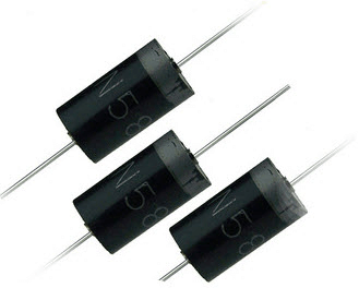
A schottky diode is an electrical component commonly known as a barrier diode. It’s widely employed as a mixer, in radio frequency applications, and in power applications as a rectifier. It’s a diode that operates at a very low voltage. In comparison to PN junction diodes, there is a lesser power drop. After the physicist Schottky, the Schottky diode was named. A hot carrier diode, a hot-electron diode, or even a surface barrier diode are all terms that have been used to describe it. This article explains what a Schottky diode is, how they’re made, what they’re used for, and what they look like.
What Is a Schottky Diode
An n-type semiconductor and a p-type semiconductor are utilized to form the p-n junction in a conventional p-n junction diode. A junction is produced between a p-type and an n-type semiconductor when connected. P-N junction is the name given to this intersection.
Metals such as aluminum or platinum replace the P-type semiconductor in Schottky diodes. Walter H. Schottky, a German physicist, inspired the Schottky diode.
A Schottky barrier diode, a surface barrier diode, a majority carrier device, a hot-electron diode, or a hot carrier diode are all terms that have been used to describe the Schottky diode. In radiofrequency (RF) applications, Schottky diodes are commonly employed.
A junction is produced when aluminum or platinum metal is combined with an N-type semiconductor. A metal-semiconductor junction, or M-S junction, is this type of connection. A Schottky barrier is a barrier or depletion layer generated by a metal-semiconductor junction between a metal and an n-type semiconductor.
The Schottky diode is substantially faster than the p-n junction diode in switching on and off. In addition, compared to a p-n junction diode, the Schottky diode creates less unwanted noise. The Schottky diode’s two features are ideal for high-speed switching power circuits.
Current flows in the forward direction when a sufficient voltage is applied to the Schottky diode. A minor voltage loss occurs across the terminals of the Schottky diode as a result of this current flow. Voltage drop is the term for this voltage loss.
The voltage drop of a silicon diode is 0.6 to 0.7 volts, while the voltage drop of a Schottky diode is 0.2 to 0.3 volts. The amount of voltage wasted to switch on a diode is known as voltage loss or voltage drop.
When a silicon diode is turned on, 0.6 to 0.7 volts are spent, whereas when a Schottky diode is turned on, 0.2 to 0.3 volts are wasted. As a result, the Schottky diode requires less voltage to operate.
The Schottky diode requires the same voltage to switch on as a germanium diode. However, germanium diodes are rarely utilized since their switching speed is much slower than Schottky diodes.
Construction of Schottky Diode
It is made up of a unilateral junction of metal and semiconductors. Gold, silver, molybdenum, tungsten, and platinum are among the metals used. Typically, an N-type semiconductor is employed, which includes Gallium. For low-frequency operation, silicon is used.
Temperature drops are directly related to Schottky diodes. Temperature doping concentration decreases and increases in N-type semiconductors. The Schottky barrier is a depletion layer that forms between the semiconductor–metal junctions.
The potential energy barrier is the name for this type of barrier. Rectifying and non-rectifying Schottky barriers are the two types of Schottky barriers. The Schottky barrier is generated when a metal and a weakly doped semiconductor collide. When a strongly doped semiconductor gets into contact with a metal in a specific order, it produces a non-rectifying barrier.
When semiconductor doping increases, the width of the depletion layer expands. When the width of the tunnel narrows, charge carriers flow through the tunnel and reach the depletion layer. The junction ceases to function as a rectifier as the doping level rises and becomes an ohmic contact.
Electrons accumulating on the semiconductor side will have a lower energy level than electrons in the metal region under unbiased conditions. Electrons are unable to pass through the Schottky Barrier due to this. When an electron on the N-side is forward biased, it obtains greater energy to pass the junction barrier and enter the metal. The electrons are also known as hot carriers because of this. As a result, the diode is known as a hot carrier diode.
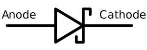
Symbol of Schottky diode
The symbol for a Schottky diode is depicted in the diagram below. The metal is the anode, and the n-type semiconductor is the cathode in a Schottky diode.
Metal-semiconductor (M-S) junction
A metal-semiconductor (M-S) junction is generated when metal is linked to an n-type semiconductor. M-S junction is a term that refers to a metal-semiconductor junction.
Non-rectifying or rectifying metal-semiconductor junctions exist. The ohmic contact is a non-rectifying metal-semiconductor connection. Non-ohmic contact refers to the rectifying metal-semiconductor junction.
What Is a Schottky Barrier?
A Schottky barrier is a depletion layer generated at metal and an n-type semiconductor junction. In basic terms, the Schottky barrier is the potential energy barrier created at the metal-semiconductor junction. Moreover, for electrons to flow across the diode, they must overcome the barrier.
- A rectifying metal-semiconductor junction forms the Schottky barrier.
- The Schottky diode is constructed using this rectifying Schottky barrier.
- A non-rectifying metal-semiconductor junction forms a non-rectifying Schottky barrier.
- The Schottky barrier height is one of the essential features of a Schottky barrier. The value of this barrier height is determined by the semiconductor and metal combination.
The Schottky barrier height of an ohmic contact (non-rectifying barrier) is very low, whereas that of a non-ohmic contact (rectifying barrier) is quite high. The barrier height is not enough to generate a depletion region in a non-rectifying Schottky barrier. As a result, in an ohmic contact diode, the depletion region is minimal or non-existent.
In the case of a rectifying Schottky barrier, on the other hand, the barrier height is sufficient to generate a depletion region. As a result, the non-ohmic contact diode has a depletion area. Compared to the ohmic contact, the non-rectifying metal-semiconductor junction (ohmic contact) has a very low resistance to electric current. Still, the rectifying metal-semiconductor junction has a very high resistance to electric current.
When gets into contact metal with a lightly doped semiconductor, the rectifying Schottky barrier is created; however, when a metal comes into contact with a severely doped semiconductor, the non-rectifying Schottky barrier is generated. The current-voltage (I-V) curve of an ohmic contact is linear, whereas the current-voltage (I-V) curve of a non-ohmic contact is non-linear.
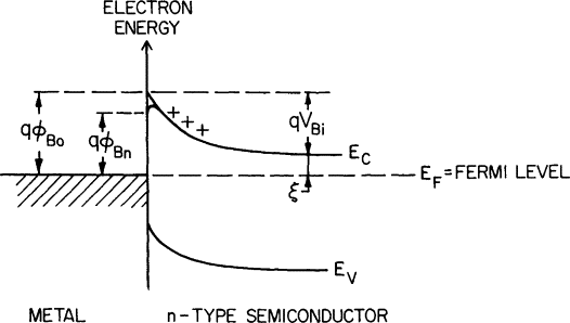
Energy Band Diagram of Schottky Diode
The figure below depicts the energy band diagram of an N-type semiconductor and a metal.
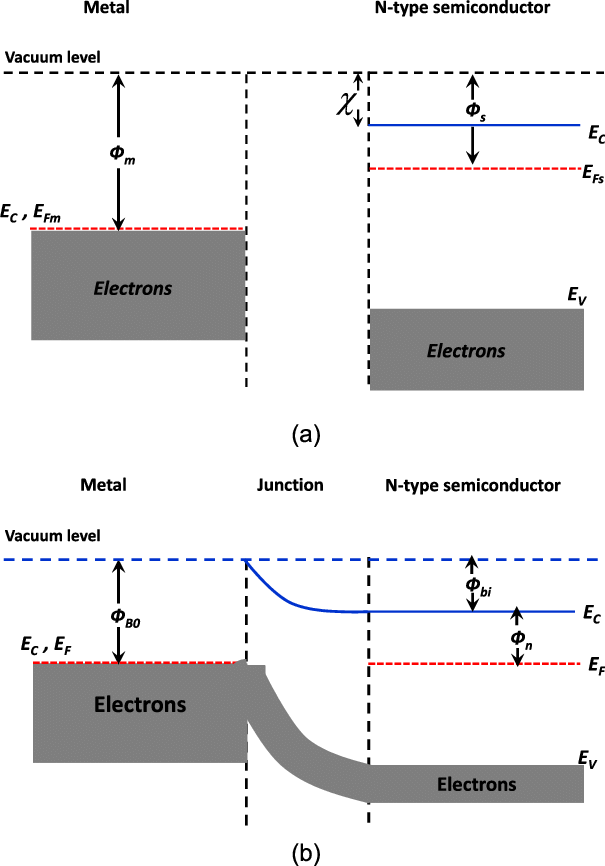
The energy level of electrons outside the material is denoted as the vacuum level. The energy amount required to transfer an electron from the Fermi level (EF) to the vacuum level (V) (E0) is defined as the work function.
Metal and semiconductor work functions are not the same. A metal’s work function is higher than a semiconductor’s work function. As a result, n-type semiconductor electrons have higher potential energy than metal electrons.
Metal and semiconductor energy levels are not the same. N-type semiconductor Fermi levels are higher than metal Fermi levels. We know that electrons at higher energies have greater potential energy than electrons at lower energies. As a result, the electrons in an N-type semiconductor have higher potential energy than those in metal.
How does the Schottky diode work?
Unbiased Schottky Diode
When the metal is linked to the n-type semiconductor, the n-type semiconductor’s conduction band electrons (free electrons) travel from the n-type semiconductor to the metal, establishing an equilibrium condition. Note a positive ion is formed when an elecron is lost from an electron atom. Additionally, if an atom acquires an additional electron, it automatically becomes a negative ion.
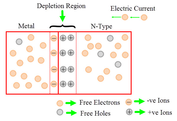
The atoms in the metal will receive extra electrons from the conduction band electrons or free electrons crossing the junction. As a result, atoms on the metal junction acquire electrons while the atoms on the n-side junction lose them.
Positive ions form when atoms lose electrons at the n-side junction, while negative ions form when atoms get extra electrons at the metal junction. As a result, positive ions form at the n-side junction, while negative ions form at the metal junction. These positive and negative ions represent the depletion zone.
The width over which these electrons flow into the metal is negligibly tiny compared to the width within the n-type semiconductor since the metal possesses a sea of free electrons. As a result, the built-in-potential or built-in voltage is mostly found inside n-type semiconductors. When the conduction band electrons of an n-type semiconductor try to go into the metal, they encounter a built-in voltage barrier.
The liberated electrons will need more energy than the built-in voltage to overcome this barrier. Only a few electrons move from n-type semiconductor to metal in an unbiased Schottky diode. The built-in voltage prevents further electron transport from the semiconductor conduction band into the metal. Energy band bending occurs near the contact when free electrons are transferred from an n-type semiconductor to metal.
Forward biased Schottky diode
The Schottky diode is forward-biased if the negative terminal on the battery is connected to the metal and the battery’s negative terminal is connected to the n-type semiconductor. Many free electrons are created in the n-type semiconductor and metal when a forward bias voltage is given to the Schottky diode. However, until the applied voltage is larger than 0.2 volts, free electrons in n-type semiconductors and metals cannot bridge the junction.
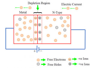
If the voltage used is adobe 0.2 volts, then free electrons accumulate sufficient energy to overcome the depletion region’s built-in voltage. As a result, the Schottky diode begins to conduct electric current. The depletion region becomes exceedingly narrow and eventually disappears if the applied voltage is repeatedly raised.
Reverse bias Schottky diode
The Schottky diode is reverse biased if the battery’s negative terminal is connected to the metal and the battery’s positive terminal is connected to the n-type semiconductor.
The depletion width widens when a reverse bias voltage is provided to the Schottky diode. As a result, the electric current comes to a complete stop. However, a nominal leakage current flows due to the thermally stimulated electrons in the metal.
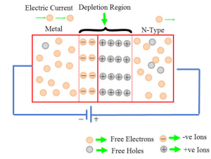
Due to the weak barrier, the electric current progressively increases as the reverse bias voltage increases. A sudden increase in electric current occurs when the reverse bias voltage is greatly raised. The depletion region breaks down due to the abrupt increase in electric current, which may irreversibly harm the device.
V-I characteristics of Schottky diode
The diagram below presents a Schottky diode’s V-I (Voltage-Current) properties. The vertical line in the diagram below shows the current flow through the Schottky diode, while horizontal line is what represents the voltage present across a Schottky diode.
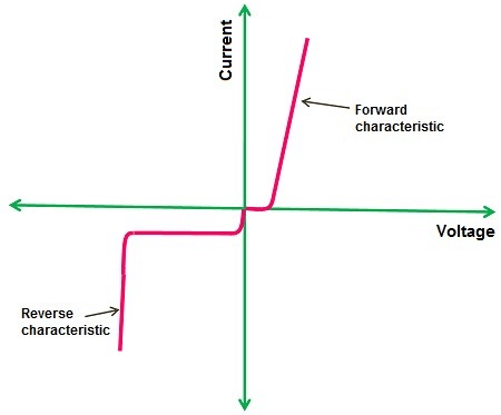
Schottky diodes have V-I properties that are almost identical to P-N junction diodes. However, compared to a P-N junction diode, the forward voltage drop of a Schottky diode is quite minimal.
Schottky diodes have a 0.2 to 0.3 forward voltage drop, whereas silicon P-N junction diodes have a forward voltage drop of 0.6 to 0.7 volts.
Electric current flows through the Schottky diode when the forward bias voltage is larger than 0.2 or 0.3 volts.
The reverse saturation current in a Schottky diode occurs at a very low voltage compared to a silicon diode.
Applications of Schottky Diode
Because of their unique features, Schottky diodes have found several applications in the electronics sector, including diode rectifiers. Below are the common applications.
RF mixer and detector diode
The Schottky diode has radiofrequency functions because of its rapid switching speed and peak frequency capacity. Schottky barrier diodes are used for high-performance diode ring mixers.
Power rectifier
Schottky barrier diodes can also be used as high-powered rectifiers. The high current density and low forward voltage drop indicate that power is wasted less than in regular PN junction diodes.
Power OR circuits
This diode might be beneficial when two distinct power sources are used to drive a load, such as in a battery supply. The power from the supply mustn’t mix with the other sources.
Solar Cell Applications
As we all know, solar cells are frequently connected to rechargeable batteries, most often lead-acid batteries, because there is power is available almost all the times. A diode would be necessary for a proportionate arrangement of solar cells because solar cells would not support the applied charge in reverse.
Conclusion
Because of their features, Schottky diodes are employed in the electronics industry for various applications in diode rectifiers. They’re engaged in voltage clamping applications to keep transistors from becoming saturated. Because digital devices demand quick switching, it is used as a Schottky TTL. Because the switching speed of diodes determines the performance of digital computers, the Schottky diode is an important component.
Lastly, for more details on Schottky diode or other electrical components, we at ICRFQ are here to help. Contact us today; we are the best electrical components manufacturer in China.
If you want to find more Electronic Components Distributors, please check out the following articles:
Electronic Components Distributors In the USA
Electronic Components Distributors In UK
Electronic Components Distributors In China
Electronic Components Distributors In India
Electronic Components Distributors In Singapore
Electronic Components Distributors In Malaysia
Electronic Components Distributors In Vietnam
Electronic Components Distributors In South Korea
- Where to buy IC chips? The Best Guide? - March 26, 2024
- Breaking Down Barriers: Overcoming Obstacles in Cross-Border Electronic Component Trade - March 4, 2024
- Everything You Need to Know About Amplifier IC Chips - March 4, 2024


