
Last Updated on October 23, 2023 by Kevin Chen
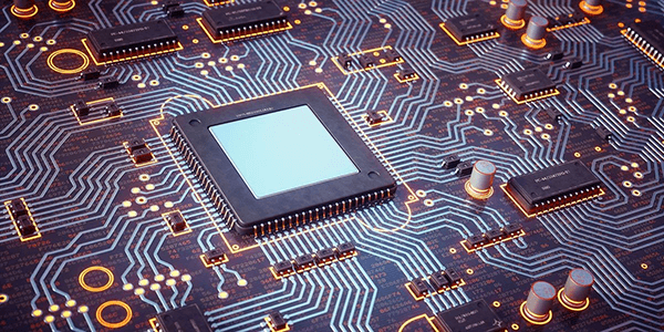
From inexpensive Silicon to rare earth elements (REEs), semiconducting materials differ in cost and availability. Semiconductors are required for the field-effect transistors, operation of solar cells, Internet of Things sensors (IoT), and self-driving car circuits. Semiconductors and the materials employed in their manufacturing are responsible for the modern world’s existence.
New materials are set to take place when conventional semiconductor materials hit their physical limits. The market for these materials, combined with new semiconductor applications, is transforming production and material procurement across the sector. This article provides an overview of semiconductor materials and a list of materials and their uses. However, first, let’s define a semiconductor.
What Is A Semiconductor?
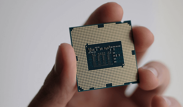
A semiconductor is a material with unique electrical properties that make it ideal for use as a basis for computers and other devices. It’s usually a compound or a solid chemical element that conducts electricity in some situations but not others. As a result, it’s an excellent medium for controlling electrical current and household appliances.
A conductor conducts electricity, while an insulator does not. Semiconductors have qualities that fall between those of a conductor and those of an insulator. Semiconductors can be found in diodes, integrated circuits (ICs), and transistors.
The conductance of a control electrode can change based on the current or voltage is given to it and the intensity of IR, UV, visible light, or X-ray irradiation. The impurities, also known as dopants added to a semiconductor, affect its unique properties.
The majority of semiconductors are built up of crystals that are made up of a variety of different materials. Users must first learn about atoms and how electrons assemble inside the atom to comprehend better how semiconductors work. Inside an atom, electrons are organized into layers known as shells. Valence shell refers to the atom’s outermost shell.
These are the electrons that make bonds with nearby atoms in this valence shell. Covalent bonds are what they’re called. The valence shell of most conductors has only one electron. In contrast, the valence shell of semiconductors usually has four electrons.
Electrons can connect with the valence electrons of other atoms if they are made of the same valence as those around them. Atoms self-organize into crystal formations whenever this happens. We use these crystals to manufacture the majority of semiconductors, mostly silicon crystals.
How Do Semiconductors Work?
Metals conduct electricity since their free electrons may freely move between atoms, which is necessary for electricity to work. Pure Silicon, for example, has very few free electrons and therefore behaves more like an insulator than a semiconductor.
Through a process known as doping, Silicon can be steered toward conductivity. Doping introduces microscopic contaminants into semiconductors. Impurities encourage conductivity by introducing “donor atoms” to the base material. Although the amount of impurities added to semiconductor materials is incredibly small—as little as one contributor atom per ten million semiconductor atoms—it is sufficient to allow electrical conductivity. N-type and P-type impurities are the two types of impurities that are used.
Phosphorus and Arsenic are two N-type semiconductors. The valence electrons of both compounds are five. When one of the doping electrons is added to the silicon lattice, it has nothing to attach to, making it available for electrical flow. These semiconductors are referred to as N-type because electrons have a negative charge.
Gallium or Boron are used to dope P-type semiconductors. The valence electrons of the two doping elements are only three. A few silicon electrons have nowhere to attach to when they mix with the silicon lattice, allowing for electrical conductivity. Silicon doped with gallium or Boron is referred to as a P-type semiconductor because it lacks an electron, which results in a positive charge.
What Are Semiconductor Materials?
Semiconductor materials have conductivity in the range between conductors and insulators. Examples include pure elements like germanium/silicon and compounds like cadmium selenide/gallium arsenide. Small amounts of impurities can be added to clean semiconductors during doping to alter the material’s conductivity drastically.
The conductivity of materials is primarily intermediate between that insulators and conductors. Semiconductors have essential features in designing solid-state devices, such as transistors and diodes.
Properties of Semiconductor Material
Semiconductor materials offer unique electrical conductivity characteristics. The success of semiconductors hinges on the ability to mass create new materials with these properties at a cost comparable to Silicon(Si).
List of Semiconductor Materials
The following is a list of semiconductor materials.
Germanium (Ge)
The semiconductor material germanium belongs to the periodic table’s group IV. This substance was employed in developing early devices such as diodes and transistors. Early transistors could face thermal runaway because diodes had a more significant temperature coefficient and reverse conductivity. It has a higher charge carrier mobility than Silicon, which is why it’s employed in some RF-based electronics.
Silicon (S)
Silicon is the most often used semiconductor material and belongs to group IV of the periodic table of chemical elements. These materials are extremely easy to work with and have excellent mechanical and electrical qualities. When these materials are utilized in integrated circuits, they produce high-quality silicon dioxide for insulation layers between the chip’s numerous active parts.
Gallium Arsenide (GaAs)
The gallium arsenide semiconductor, which belongs to the III-V periodic table group, is the most frequently utilized material after Silicon. It is widely employed in high-performance RF devices that use this element’s strong electron mobility. It’s also a substrate in other III-V semiconductors like GaInNAs and InGaAs. When compared to Silicon, this material exhibits reduced hole mobility. It’s also difficult to make, which raises the cost of GaAs devices.
Silicon Carbide (SiC)
Silicon carbide is a periodic table element belonging to the IV group. Compared to Si-based devices, these components are used in power electronics because they have lower losses and higher operating temperatures. When compared to Silicon, this material has a ten-fold higher breakdown capacity. In blue and yellow LEDs, silicon carbide material types are used.
Gallium Nitride (GaN)
In the periodic table, gallium nitride, or GaN, is a member of the III-V group. It’s most commonly found in microwave transistors and ICs, where maximum power and temperatures are necessary. This semiconductor material is challenging to dope to produce p-type areas and is electrostatically responsive but not ionizing radiation sensitive. Blue LEDs have been made from this material.
Gallium Phosphide (GaP)
Gallium Phosphide, or GaP, is a semiconductor material belonging to the III-V periodic table group. This material is utilized in early low-to-medium-brightness LEDs that generate multiple colors depending on the number of dopants used. Pure GaP produces green light, nitrogen-doped GaP produces yellow-green light, and ZnO-doped GaP has a red light.
Cadmium Sulphide (CdS)
Cadmium sulfide, or CdS, is a semiconductor material that belongs to the II-VI group of the periodic table. Solar cells and photoresistors both employ this substance.
Lead Sulphide (PbS)
The semiconductor substance Lead Sulphide, also known as PBS, is an IV-VI group element in the periodic table that was used in early radio detectors called Cat’s Whiskers, which used a tip contact made by placing a thin wire on the galena to provide signal rectification.
Types of Semiconductor Material
There are two different types of semiconductor materials, as shown below.
Intrinsic Semiconductor Material
One of the critical features of an intrinsic semiconductor material is that it is chemically very pure. As a result, it has a lower conductivity level and a lower number of charge carriers, such as electrons and holes, in equal proportions.
As an alternative to contaminants, the number of charge carriers in this semiconductor material can be determined by the material parameters. As a result, the number of charged electrons equals the number of holes (n = p), resulting in i-type semiconductors or undoped.
Si and Ge are the most often utilized intrinsic semiconductor materials, and they have four electrons in their valence shell, making them tetravalent. These two minerals belong to the IVth Group of the periodic table, and their atomic numbers are 14 and 32, respectively.
Extrinsic Semiconductor Material
Extrinsic semiconductor materials are created by mixing a small number of impurities with the intrinsic semiconductor material. The bandgap of this material can be adjusted by doping it with tiny impurities.
This ‘doping’ uses an element from the periodic table to make the semiconductor’s valence band contain either fewer or more electrons than the semiconductor itself. As a result, either scarcity or surplus of electrons will result.
P-Type extrinsic semiconductors and N-type extrinsic semiconductors are two forms of extrinsic semiconductor materials that are categorized based on the type of additional impurity.
P-Type Extrinsic Semiconductor
A small quantity of trivalent impurity can be added to a pure semiconductor to produce a P-type extrinsic semiconductor. Three valence electrons are present in the impurity that is added. When an atom similar to Boron (B) is introduced to a germanium (Ge) atom, three valence electrons are coupled to the germanium atoms, forming three covalent connections. Another electron in the Ge atom, on the other hand, will remain without creating a link. The space is referred to as a hole when an atom lacks an electron to form a covalent bond.
N-Type Extrinsic Semiconductor
A little quantity of pentavalent impurity can be added to a pure semiconductor to create an N-type semiconductor. As a result, this impurity contains five valence electrons.
For example, if an atom similar to Arsenic is added to the ‘Ge’ atom, 4 valence electrons will be bonded through the germanium atoms, while one electron will remain free.
What Are The Most Used Semiconductor Materials?
Germanium, Silicon, and gallium arsenide are the most common semiconductor materials. Germanium has electrons of four valence electrons that are placed on the atom’s outer shell.
The quantity of valence electrons present determines the conductivity of semiconductor material. While Germanium was a crucial stage in the history of semiconductor materials, it has mostly fallen out of favor with Silicon, the most commonly used semiconductor material.
Since the 1950s, Silicon has been widely used in semiconductors. After carbon, Silicon is the most prevalent element on the planet, with four valence electrons and a greater melting temperature.
Quartzite has a high concentration of Silicon. Silicon purification, extraction, and crystallization are all effective and cost-effective techniques. Because Silicon crystallizes in a diamond structure for a relatively stable connection, it has excellent mechanical qualities.
Gallium arsenide is the world’s second most popular semiconductor. Gallium arsenide, unlike Germanium and Silicon, is a chemical created by mixing gallium, which has 3 valence electrons, and Arsenic, which has 5.
Gallium-arsenide semiconductors respond quickly to electric signals because they have eight valence electrons, making them ideal for amplifying high-frequency signals like those found in television satellites. However, gallium arsenide has several drawbacks: it’s more challenging to mass-produce than Silicon, and the chemicals required to make it are extremely poisonous.
What Are Some Of The Most Recent Semiconductor Material Innovations?
Silicon, the essential raw material in semiconducting manufacturing for the majority of the beginning of the twenty century, is nearing the end of its useful life. Industry analysts fear that Silicon will soon reach the boundaries of Moore’s Law due to demands for ever-smaller, quicker integrated circuits. New materials are still being researched, with some showing tremendous potential in the future:
● Given the high critical energy field, high-power gallium nitride can be utilized in electric grid systems for more efficient and faster power conversions.
● Improved infrared sensors for the military and medical sectors use bismuthide and antimonide-based semiconductors.
● Although graphene has the potential to overtake Silicon as an all-purpose semiconductor material, mainstream commercialization could take up to twenty-five years.
● Pyrite can replace cadmium telluride, a rare earth element widely utilized in solar cells but has a limited supply. Pyrite is a mineral that is abundant, harmless, and affordable.
What Are The Characteristics Of Semiconductor Materials That Set Them Apart?
As the name suggests, conductors are materials that allow for electrical conduction. Silver, Gold, and copper are a few examples. Insulators, on the other hand, have a solid resistance to electricity and prevent it. Insulators include glass, rubber, and ceramic.
Semiconductors have both conductivity and insulator properties, as their name suggests. Semiconductors are usually crystalline and have a low amount of free electrons, which is required for conductivity. Instead, their atoms create a crystal lattice that allows for electrical conductivity, but only under certain conditions.
Semiconductors are insulators at low temperatures, allowing little or no conductivity. However, they can conduct electricity at room temperature and when subjected to light, voltage, or heat. Semiconductors are vital in electrical devices because they govern how, when, and where electricity flows because of this quasi-state between conductors and insulators.
How Are Semiconductor Materials Manufactured?
Circuit components like transistors and wires are placed on the surface of thin silicon crystal wafers when integrated circuits are produced. The circuit pattern is subsequently projected using the photolithography technique onto the thin component film, which is coated with a photo-resistant material.
As a result, a single circuit layer is formed, with transistors at the bottom. The step is repeated with many circuits built on top of each other and semiconductor base.
Applications of Semiconductor Materials
Almost all electronic gadgets rely on semiconductor production for their basic hardware. It’s utilized for energy amplification, Switching, energy conversion, and sensors, among other things.
What Are The Most Common Goods Manufactured From Semiconductor Materials?
The following are examples of standard semiconductor-based products and components:
- Bipolar Transistors
- Diodes
- Field-Effect Transistors
- IC
- Junction Field-Effect Transistor
- LEDs
- MOSFETs
- Silicon-Controlled Rectifiers
What Industries Make The Most Use Of Semiconductor Materials?
Semiconductor materials are significant for all major businesses since they are critical electronic equipment components. Over a hundred billion semiconductors are used every day around the world. The following industries are particularly reliant on semiconductor materials:
- AI
- Clean Energy
- Information and Communication
- Computing Industries
- Energy industries
- Health Care industries
- IoT
- Military
The market for Semiconductor Materials
The semiconductor market is pretty stable because electronic gadgets are used practically all industrial areas. The materials needed for early semiconductor packaging production range from cheap Silicon and ceramic to expensive rare earth metals.
What Gives Semiconductor Materials Their Value?
While some semiconductor materials are both inexpensive and plentiful—Silicon as an obvious example—the REE utilized in manufacturing high-dielectrics, and chemical/mechanical polishing can be expensive.
REE value is affected by several things. Separating REEs from the rock is a time-consuming and expensive process that involves hundreds of steps to remove and purify the ultimate product.
Many mining corporations have opted not to pursue REE earnings due to the difficulties of obtaining REEs from raw minerals. China is one of the few countries that focus on REE mining and processing, providing 85 percent of the world’s tungsten and molybdenum supply.
Because of China’s monopoly on REE manufacturing, it can control pricing and use the lucrative semiconductor material as a political tool.
What Methods Are Used To Recycle And Reclaim Semiconductor Materials?
Recycling and recovering valuable REE and other chemicals are options, given the worth of some semiconductor materials. Regarding large-scale semiconductor goods like car catalysts, solar cells, and wind turbine magnets, REE recycling is now the most successful. Batteries can also be salvaged for REEs.
Given the limited amount of material retrieved from specific goods, such as cellphones, recycling small semiconductor materials is a cost challenge. Recycling semiconductor materials comes with environmental costs: it generates a lot of waste and emits many harmful chemicals. Many discarded semiconductor goods end up in third-world e-waste recycling operations infamous for exploiting child labor, which raises ethical concerns.
The simplest method to lower REE costs is for countries other than China to start mining and refining their REE reserves. However, as noted in Communications of the ACM, this necessitates a willingness to spend on developing extraction, cost-effective mining, and refining methods.
Semiconductor Material Parameters
Information regarding semiconductor materials must be available when developing ICs and electronic devices. The semiconductor material must be differentiated in terms of different properties such as electrical, optical, and thermal before the production process can begin.
The kind of mobility, conductivity, resistivity, concentration and carrier lifespan are essential characteristics. The light absorption coefficient, energy gap of semiconductors, refraction index, and impact ionization coefficient are other additional factors.
Applications Of Semiconductor Materials
The applications of semiconductor materials include the following.
- Semiconductor materials are employed in producing various electronic components found in electronic gadgets.
- Sensors, Switching, amplification, energy conversion, and other applications need for these materials.
- Junction field-effect transistors, diodes, integrated circuits, field-effect transistors, bipolar transistors, MOSFETs, LEDs, Silicon-Controlled Rectifiers, and other semiconductor materials are used to make standard components and products.
- Electronic gadgets used in almost every industry require semiconductor materials. Semiconductor materials are used in various industries, including energy, artificial intelligence, clean energy, communication, computer, the military, health care, and the Internet of Things.
Last but Not Least
Semiconductor materials are used to make many modern electronic components. A semiconductor material’s electrical conductivity is halfway between a good conductor like copper and an excellent insulator like glass, hence the name.
A semiconductor, on the other hand, can act as a conductor or an insulator depending on the electrical conditions. The remarkable electrical characteristics of semiconductors are used in most modern electronics.
Semiconductor materials have a usual molecular structure known as a lattice, which results in strong bonding pairs of valence electrons among neighboring atoms in the lattice, solid, resulting in a durable, crystalline material. Solid-state electronics are differentiated from older thermionic-based electronics that use vacuum tubes and other technology. Germanium (Ge) and Silicon (Si) are two common semiconductor materials.
Semiconductors are made pure but with tiny portions of accurately added impurities of other elements or compounds called dopants when fabricating electronic components.
Conclusion
This article is about semiconductor materials, types, and applications in general. We know that different semiconductor materials exist, but Silicon, or Si, is the most commonly used over Germanium in various electronics and semiconductor applications. This is because the energy band gap of Si is 0.7eV, the production of thermal pairs is smaller, Si is readily available in nature, less noise, and SiO2 formation is simple. As a result, Silicon is used to make a variety of electronic components such as switches, resistors, capacitors, diodes, transistors, and other components used in various circuits.
For more details on Semiconductors and electrical components, contact us at ICRFQ. We manufacture the best electrical components in China.
If you want to find more Electronic Components Distributors, please check out the following articles:
Electronic Components Distributors In the USA
Electronic Components Distributors In UK
Electronic Components Distributors In China
Electronic Components Distributors In India
Electronic Components Distributors In Singapore
Electronic Components Distributors In Malaysia
Electronic Components Distributors In Vietnam
Electronic Components Distributors In South Korea
- Where to buy IC chips? The Best Guide? - March 26, 2024
- Breaking Down Barriers: Overcoming Obstacles in Cross-Border Electronic Component Trade - March 4, 2024
- Everything You Need to Know About Amplifier IC Chips - March 4, 2024


