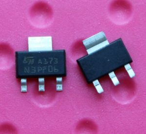
STN3PF06
Part Number: STN3PF06
Manufacturer: STMicroelectronics
Description: MOSFET P-Ch 60 Volt 2.5 Amp
Shipped from: Shenzhen/HK Warehouse
Stock Available: Check with us
ICRFQ.com - Electronic Components Distributor in China Since 2003

We make your sourcing easier!
Get A Fast Quote Worldwide!

Part Number: STN3PF06
Manufacturer: STMicroelectronics
Description: MOSFET P-Ch 60 Volt 2.5 Amp
Shipped from: Shenzhen/HK Warehouse
Stock Available: Check with us
| Datasheet | |
|---|---|
| Category | Discrete Semiconductor Products |
| Family | Transistors – FETs, MOSFETs – Single |
| Manufacturer | STMicroelectronics |
| Series | STripFET? II |
| Packaging | Tape & Reel (TR) |
| FET Type | MOSFET P-Channel, Metal Oxide |
| FET Feature | Standard |
| Drain to Source Voltage (Vdss) | 60V |
| Current – Continuous Drain (Id) @ 25°C | 2.5A (Tc) |
| Rds On (Max) @ Id, Vgs | 220 mOhm @ 1.5A, 10V |
| Vgs(th) (Max) @ Id | 4V @ 250μA |
| Gate Charge (Qg) @ Vgs | 21nC @ 10V |
| Input Capacitance (Ciss) @ Vds | 850pF @ 25V |
| Power – Max | 2.5W |
| Operating Temperature | -65°C ~ 150°C (TJ) |
| Mounting Type | Surface Mount |
| Package / Case | TO-261-4, TO-261AA |
| Supplier Device Package | SOT-223 |
The power MOSFET, known as STN3PF06, will be the topic of today’s discussion. Some of you may be asking what exactly a power MOSFET is. Please allow me to jog your memory a little bit.
Power MOSFETs make use of semiconductor processing methods comparable to those used in present-day VLSI circuits, with the exception that the levels of device voltage and current are very different from one another. The field-effect transistor (FET) introduced in the 1970s is the primary inspiration for the MOSFET. Because of the limitations of BJTs, the power MOSFET was invented, and at the moment, this device is the one that is most commonly used in power electronics applications.
Even though it is impossible to categorize a power device’s operating limitations thoroughly, power devices can be referred to as any component that can switch at least 1A of current. This makes it impossible to classify the operational limits of a power device.
One type of device that regulates the current supply is the bipolar power transistor. The base drives current needs to be relatively high compared to one-fourth of the collector current for the device to remain in the ON state. Additionally, to obtain a speedy turn-off, it is required to use sizeable reverse base drive currents. An introduction to power MOSFETs and how they work is provided in the following article.
The term “Power MOSFET” refers to a specific variety of MOSFET capable of managing large quantities of power. The switching speed of these MOSFETs is much faster than that of regular MOSFETs operating in lower voltage ranges, which allows them to function far more effectively. It works in the same way standard MOSFETs do regarding their working principle.
The p-channel enhancement mode, the n-channel enhancement mode, the n-channel depletion mode, and the p-channel depletion mode are the power MOSFETs utilized most frequently. The frequency of the power MOSFET can reach up to 100 kilohertz at its highest point.
These three-terminal silicon devices send a signal to the gate terminal to control current conduction between the source and drain terminals. The gate terminal receives the signal. The current conduction capacity is equivalent to thousands of amperes, and the breakdown voltage values range from ten to one thousand volts.
In addition, power MOSFETs can be purchased in a variety of architectures, including VDMOS (Vertical Diffused MOS), DMOS (Double-Diffused MOS), Trench-MOS (UMOS), or VMOS, amongst others.
The power MOSFET used in integrated circuits is a lateral device with source, drain, and gate terminals on the apex of the device. This creates a situation where the current flowing within a lane parallels the current flowing on the device’s exterior. The substrate of a device serves as the drain terminal for the VDMOS, also referred to as the Vertical Double Diffused MOSFET.
MOSFETs used in IC will have a higher on-resistance than discrete MOSFETs. Power MOSFETs can be purchased in small outline integrated circuit, or SOIC, packages. These packages are put to use in situations where there is a limited amount of space. Additionally, TO-247, larger through-hole TO-220, and surface mountable D2PAK or SMD-220 are available.
Chip-scale devices, in addition to the PolarPakTM and DirectFETTM packages, are examples of more recent packaging options. The manufacturing technique that is utilized in the production of power MOSFETs is comparable to the manufacturing process that is used in the production of VLSI circuits; however, the levels of voltage and current are distinct.
Altering the voltage on the gate terminal causes these variants of MOSFETs to switch and regulate the flow of current between two terminals, such as source and drain, in a manner that is analogous to that of conventional MOSFETs. After the voltage has been applied to the gate terminal, a channel will be able to form between the source terminal and the gate terminal, which will allow current to flow through the device.
When a MOSFET is utilized in the function of a switch, it operates in ohmic ranges and turns off when the ON/OFF state is reached. In the saturation region, it is feasible to omit the method to reduce the power loss while the operating condition is in place. This is achievable because the saturation region has a higher power density.
When the gate-source voltage drops below the threshold voltage, the power MOSFET will move into the cut-off section of its operating range. This condition is present when the threshold voltage is lower than the gate-source voltage. To prevent a breakdown, the voltage between the drain and the source must have a breakdown voltage higher than the voltage being applied to the circuit. As a direct consequence of this, an avalanche breakup will occur.
Once the power MOSFET enters the ohmic state, the amount of power lost due to dissipation drops to a barely detectable level. When saturation has occurred, the drain-to-source voltage has minimal effect on the drain current. The voltage between the gate terminals and the source terminals is the sole factor determining its behavior. When contrasted with the voltage that is present at the threshold, the voltage that is present at the gate terminal is noticeably higher. The drain current will increase when there is a larger voltage differential between the gate and the source.
This Power MOSFET is STMicroelectronics’ most recent advancement of their proprietary “single feature size” strip-based technique. The final transistor has outstanding manufacturing reproducibility thanks to its low on-resistance, tough avalanche properties, and lack of crucial alignment stages.
Hopefully, you’ve picked up some new information today. Feel free to ask questions in the comments box below this article or any other topic on our site.
Contact ICRFQ for pricing on STN3PF06 or any other electronic component. We are the leading supplier of electronic components in China.
WhatsApp us