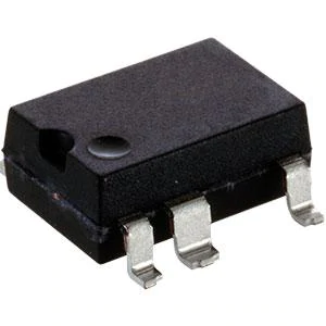
TOP243GN
Part Number: TOP243GN
Manufacturer: Power Integrations
Description: AC/DC Converters 15W 85-265 VAC 25W 230 VAC
Shipped from: Shenzhen/HK Warehouse
Stock Available: Check with us
ICRFQ.com - Electronic Components Distributor in China Since 2003

Part Number: TOP243GN
Manufacturer: Power Integrations
Description: AC/DC Converters 15W 85-265 VAC 25W 230 VAC
Shipped from: Shenzhen/HK Warehouse
Stock Available: Check with us
| Datasheet | |
|---|---|
| Category | Integrated Circuits (ICs) |
| Family | PMIC – AC DC Converters, Offline Switchers |
| Manufacturer | Power Integrations |
| Series | TOPSwitch?-GX |
| Packaging | Tube |
| Part Status | Active |
| Output Isolation | Isolated |
| Internal Switch(s) | Yes |
| Voltage – Breakdown | 700V |
| Topology | Flyback |
| Voltage – Start Up | – |
| Voltage – Supply (Vcc/Vdd) | – |
| Duty Cycle | 66.5% |
| Frequency – Switching | 66kHz ~ 132kHz |
| Power (Watts) | 25W |
| Fault Protection | Current Limiting, Over Temperature, Over Voltage |
| Control Features | Frequency Control |
| Operating Temperature | -40°C ~ 150°C (TJ) |
| Package / Case | 8-SMD (7 Leads), Gull Wing |
| Supplier Device Package | SMD-8B |
| Mounting Type | Surface Mount |
Using the same tried-and-true topology as TOPSwitch, the TOP243GN is an expanded power design flexible EcoSmart® Integrated Offline Switcher that incorporates the high voltage power MOSFET, PWM control, fault protection, and other control circuitry into a single CMOS chip. The design’s adaptability, performance, and energy efficiency are all boosted by the consolidation of numerous features. This chip is a high-voltage switched-mode power supply that takes an input current and converts it into a duty cycle that controls the open drain of a power MOSFET. The power MOSFET’s duty cycle drops linearly with increasing current over its CONTROL pin under normal conditions. It has several extra features that boost the power supply’s efficiency and adaptability to different designs. All of the low-voltage control circuitry and the high-voltage power MOSFET can be efficiently combined into a single monolithic chip using a unique high-voltage CMOS technology.
All accessible package versions have soft-start, 132 kHz switching frequency (automatically lowered at light load), and frequency jittering for lower EMI, hysteretic thermal shutdown, broader DCMAX, and higher creep age.
Tighter temperature and absolute tolerances have been applied to all critical parameters (including current limit, frequency, and PWM gain) to further ease design and optimize system cost.
In order to manage the duty cycle of a high voltage power MOSFET at the open drain output, the TOPSwitch and TOPSwitch-GX integrated switched mode power supply chips require a control input current.
The TOPSwitch-GX can be used in a three-terminal mode similar to the original TOPSwitch by connecting these terminals to the SOURCE pin. But even in this three-terminal mode, the TOPSwitch-GX has several new transparent functions that don’t require any more hardware:
By connecting a resistor from the LINE-SENSE (L) pin to the rectified DC high voltage bus, you can sense line voltage and utilize that information to implement features like line overvoltage (OV), undervoltage (UV), and line feed-forward with DCMAX reduction. Here, the OV/UV cutoffs are set by the resistor’s value, and the DCMAX drops off linearly after the line voltage rises above the UV cutoff.
The Function of the CONTROL (C) Pin With its low impedance, the CONTROL pin may accept both supply and feedback currents. A shunt regulator is used to separate the feedback signal from the power current when the system is running normally. The supply voltage for the control circuitry, which includes the MOSFET gate driver, is the voltage at the CONTROL pin (VC). Instantaneous gate drive current must be supplied by an external bypass capacitor connected in series with the CONTROL and SOURCE pins. Both the auto-restart interval and the control loop compensation are determined by the total capacitance attached to this pin. Starting with the MOSFET turned off and a DC high voltage source connected to the DRAIN pin, a switching high voltage current source charges the capacitor connected to the CONTROL pin. Initiating the soft start occurs when the voltage on the CONTROL pin, denoted by VC, hits roughly 5.8 V. Over the course of about 10 ms, the soft-start circuit raises the MOSFET’s duty cycle from zero to its maximum value.
The high voltage current source is shut off at the end of the soft start, and the CONTROL pin begins discharging in response to the supply current pulled by the control circuitry if no external feedback/supply current is provided into the pin. In a well-designed power supply, the CONTROL pin voltage won’t drop below the lower threshold voltage of about 4.8 V before the feedback loop closes and supplies external CONTROL pin current. This assumes no fault conditions, such as an open loop or a shorted output (internal supply under-voltage lockout threshold). While the CONTROL pin of the shunt regulator is being charged by an external current source.
5.8 V; any current in excess of the chip’s needs is sent back to SOURCE via RE. As the current flows through RE, the duty cycle of the power MOSFET is regulated, allowing for closed-loop control. The gain of the error amplifier is controlled by the shunt regulator’s finite low output impedance ZC in a main feedback mode. The control loop’s dominant pole is determined by the CONTROL pin’s dynamic impedance ZC and the external CONTROL pin capacitance.
If you require any information or would like to place an order for the KSZ8081RNBIA-TR, please contact ICRFQ, your one-stop shop for electronic sourcing components in China. We are committed to putting in the effort necessary to ensure that you are provided with the highest quality goods at the most competitive pricing.
WhatsApp us