
Last Updated on April 10, 2022 by Kevin Chen
The PCB market is rapidly expanding to satisfy the needs and requirements of various electronic and electrical devices. Examples include ceramic PCBs, metal OCBs, and even transparent PCBs.
Whether you believe it or not, the PCB market has changed dramatically with the introduction of transparent glass technology. Transparent PCBs are used in a variety of LCD and LED products. However, its employment in a 5G network is the most promising of its applications. This will undoubtedly alter the way people communicate forever.
The translucent PCB can have a luminescence of 360 degrees and a rendering index of 140lmw or more. A heat sink and light attenuation are not required. Take your time and read through our guide on transparent PCBs if you want to stay current with the rest of the world by learning about the latest sophisticated printed circuit boards.
What is a Printed Circuit Board?
A PCB is an electronic circuit that provides a conduit for electronic components and mechanical support in a device. PCBs are utilized in internal computer components such as expansion cards, network interface cards, controller cards, and video cards in laptops and desktop computers. The motherboard, also a printed circuit board, connects all components.
PCBs are utilized in a variety of electronic devices in addition to computers. One or more PCBs are found in most digital cameras, televisions, digital cameras, tablets, and cellphones.
How are Printed Circuit Boards Made?
Copper is used to making PCBs. The copper is plated onto a substrate and then sliced to reveal the board’s unique design. Because there are so many layers, they must be linked correctly and integrated to ensure a solid fit.
PCB designers have concentrated on designing PCBs that are sturdy, compact, and capable of incorporating electrical power. PCBs have progressed to the point where they are currently used in ordinary electrical consumer devices.
PCB materials – PCBs are made up of various components and substrates. Different material selections will give circuits of variable quality that permit performance in specific circumstances; hence, material selection depends on material needs.
Designers frequently select materials based on electrical performance for high thermal endurance, high-speed applications, or mechanical performance for applications such as automotive under the hood.
PCB designers face various performance characteristics when it comes to material selection for their designs. The following are some of the most typical considerations:
- Mitigated loss factors
- Flame retardance
- Dielectric constant
- Thermal performance
- Dimensional stability
PCB Layout Design
To set, there was just one default trace clearance and width rule. Designers are in charge of manually altering the width of ground and power nets and controlling any additional net requirements. For firms requiring more clearances than the default amount, designers either adjust the grid or reset the value and add spacings around the layer in the graphics portion for visual reference.
It’s critical to ensure that the rules placed into the schematic are translated precisely and appropriately into the layout. When it comes to power, it’s common to add restrictions that weren’t originally in the schematic.
The manufacturing and mechanical clearance rules have been included in the equation.
PCBs come in a variety of varieties, including:
- Rigid PCBs
- Flex PCBs
- Double-Sided PCBs
- Single-Sided PCBs
- Rigid-Flex PCBs
- Multilayer PCBs
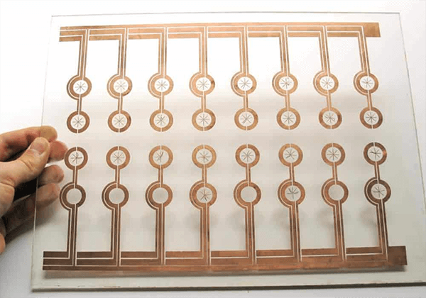
Transparent PCB Substrate
Transparent PCBs can be made from two different substrates. Either ceramic or Glass is used. Compared to Glass, ceramic, transparent PCB substrates have a high thermal conductivity. It does, however, have a lesser transmissivity. It has a transmissivity of 75 to 85%, whereas Glass has a transmissivity of 99.5 to 99.99%
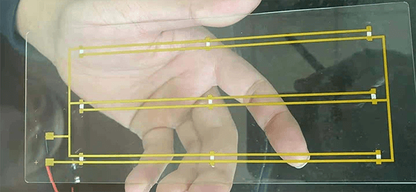
Transparent Glass PCB
Let’s take a quick look at what Glass is and how it’s used in the printed circuit board business before we get into the uses and description of transparent PCBs. Glass is typically manufactured from soda, limestone, ash, and sand. These four materials are usually recyclable, making them environmentally friendly.
- Tempered Glass is also known as reprocessed and pre-stressed Glass. This increases the longevity of the product. Furthermore, its stress absorbing and impact resistance are usually stronger and essential in extreme instances. Sapphire glass is by far the hardest and strongest material on the planet.
- Sapphire glass is used in many high-end and sophisticated electronics because of its high dielectric and thermal characteristics. Even in satellite and space gadgets and technology, it has applications.
- Now that we’ve learned a lot about Glass and its components let’s focus on transparent PCBs. Printed circuit boards made of transparent Glass are what these are. They also have a 360-degree illumination system. As a result, the light will be able to pass through, providing illumination from all sides.
- Using Glass as a substrate has certain distinct advantages. Tear resistance, heat resistance, deformation, transparency, flatness, and other properties contribute to these advantages. The deformation rate is exceptionally low at high temperatures and after working for lengthy periods.
This is one of the reasons why it is used to beautify so many things. However, one significant advantage, and possibly the biggest, is their invisible wire ornamentation. This significantly increases the device’s worth.
Benefits of Transparent Glass PCBs
Glass is already a cutting-edge material. Using transparent printed circuit boards will undoubtedly add value to circuit board constructions. PCBs that are transparent are not excluded.
Transparent PCBs allow light to pass through. As a result, the transparent PCB becomes more versatile and better. Transparent glass PCBs are also often flat. This indicates that it will have excellent symmetry and fewer defects. This improves the gadgets’ efficiency and durability.
These transparent PCBs are also heat and temperature resistant. Glass can resist up to 1000 degrees Fahrenheit temperatures. Furthermore, it is simple to manufacture large quantities of PCBs and semiconductors.
Glass translucent PCBs are simple to produce. This is since Glass can be made from recycled materials such as sand and ash. As a result, transparent glass PCBs are less expensive than ceramic PCBs. As a result, Glass transparent PCBs will reduce the cost of manufacturing all of your devices.
Thanks to heat, dust, and water resistance, the deformation rating of Glass is the least. This ensures that transparent glass PCBs can withstand use for a long time, even in extreme conditions.
To make this type of transparent PCB, heat sinking is not required. As a result, the rate of manufacturing is increased even more.
Copper Traces on the PCB are not transparent, even though the glass PCB substrate is. As a result, the copper traces on the PCB can be seen through the Glass. Some manufacturers, however, are employing new technology that allows copper traces to be transparent in the same way as glass substrates are.
Glass PCBs exposed to high temperatures for lengthy periods show extremely little deformation due to the features of the glass substrate. One of the most attractive properties of glass substrates for PCBs is this. Glass can endure temperatures of up to 1000°C, and transparent PCBs are simple to make due to the abundance of raw materials. Glass PCBs are also less expensive than ceramic PCBs as a result of this.
Transparent Ceramic Circuit Boards
Various materials like Al-Mg spinel, Aron, yttrium oxide, magnesium oxide, and alumina or aluminium oxide manufacture translucent ceramic circuit boards. For example, they employ nano-sized alumina powder in resin water solutions at a 5 to 10% concentration. The resin hardness is increased from 6H to 8H due to this. Some producers use oil-based alumina liquid to make translucent ceramic circuit boards, while others use water-based alumina liquid.
Most transparent ceramic PCBs employ transparent substrates with a glass solder mask. The conductors, on the other hand, are opaque. The transparency of the transparent substrate is between 75 and 85 percent. The traces are covered with a glass solder mask, which helps to keep the substrate transparent.
Advantages of Transparent Ceramic Circuit Boards
● It has numerous optical characteristics.
● An example is an extremely high-temperature resistance, such as temperatures of 2000°C or above. Thorium oxide and yttrium oxide circuit boards may achieve temperatures of 3100 degrees Celsius.
● Thermal conductivity ranges from 24 to 31.4 W/MK.
● The thermal expansion coefficient is relatively low and constant.
● Excellent electrical insulation • Minimal water absorption
● Applications of Transparent Ceramic Circuit Boards
● Optical sensors, high-power LEDs, high-pressure sodium vapor lamps, and infrared windows in missiles and aircraft are all examples of applications for transparent ceramic circuit boards.
Transparent Flexible PCBs
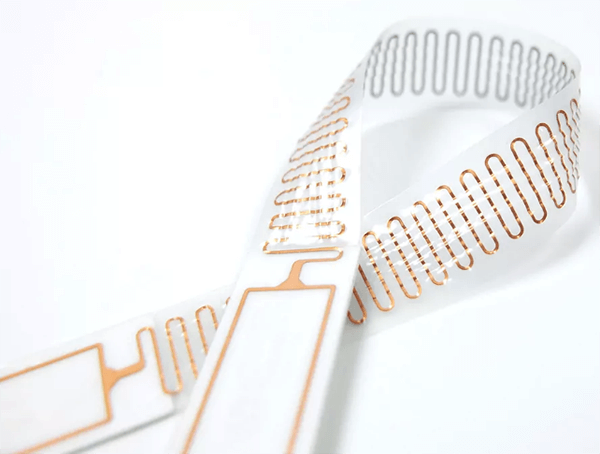
Flex and flex-rigid printed circuit boards are increasingly being employed in many products due to their multiple advantages (cost, space, and weight economies). The transparent printed circuit board is another interesting form of the flexible printed circuit board.
The system is incredibly flexible, and the substrate is only a few microns thick, thanks to polyimide as the base material.
Flexible circuits are utilized in instrument panels, underbody controls, circuits hidden in the cabin headliner, and ABS systems in the car industry. Flexible circuits are utilized on the moving printhead of printers to connect signals to the moving arm that carries the read/write heads of hard disk drives in computer peripherals.
Flexible circuits are used in consumer electronics devices such as cameras, cellphones, calculators, and training monitors. Flexible circuits are also used in industrial and medical devices and anywhere where many connections must be made in a small space.
Advantages of Transparent PCBs (Flexible)
Some of the advantages of flexible transparent PCBs are listed below.
They have a lot of cool optical features.
They are flexible, twistable, foldable, arbitrarily moveable, and bendable in three-dimensional spaces.
Achieve product thinning, miniaturization, and lightness
Compared to rigid printed circuit boards with identical quantities, flexible printed circuits save roughly 90% of the product’s weight. The manufacturing accuracy of this transparent PCB reaches the nano or micro level.
Transparent Flexible PCB Applications
The following are some of the applications for transparent flexible circuit boards: ABS systems, mobile phones, cameras, instrument panels, automatic control, medical equipment, and other locations where connections are needed in tight spaces use flexible transparent circuit boards. Electronic devices, contact lenses, and electronic skins can benefit from flexible PCBs that are completely transparent.
Transparent PCB Board Design
Circuit Design Preparation
The transparent PCB Board can be designed on a variety of platforms. You can make use of the “EASYeda” software. This software is free to use, simple to learn, and the components are easy to locate.
Create a schematic diagram for that circuit after that. After that, you’ll utilize the autoroute tool to route your circuit’s paths, after which you’ll model the layout of your PCB. This step may appear complicated to newcomers. However, you should get by with only a few lessons.
Some component diagrams and texts are unwelcome. We require the pads and tracks for transparent PCB boards. So, if you’re happy with the design, isolate the pads and oaths layers in your layer palette, then save the image as a PNG file.
It is necessary to employ a negative photoresist. The resist must be exposed to light to work. As a result, you’ll want to use the “white on black” option for the dialog you’re exporting.
Transparent PCB Board Design Printing
You should have received the exported picture that you designed by now. The goal of the OHP print is to create a mask that prevents UV light exposure in areas where it is not desired. To accomplish this, the black parts of the OHP print must effectively block light.
However, if this is not the case, the light will leak. A single print layer will not be enough to obscure the light properly. As a result, align three prints before placing them on top of each other. Also, use adhesive to keep them in place.
Gluing Your Copper Foil to Glass
We’ll now glue your copper foil to the Glass. The undesired copper will have to be removed during the final steps. This is accomplished through the use of ferric chloride to dissolve it. Choose a thick copper foil to make the entire process take longer. It’s fine to use one that’s only 0.05 mm thick.
Conclusion
According to Rush PCB USA, the PCB sector is undergoing multiple revolutionary developments. To meet the needs and specifications of various electrical devices, manufacturers use a variety of inventive ways. The creation of translucent PCBs is one of these cutting-edge processes. Transparent PCBs will become increasingly popular as 5G, LCDs, and LEDs become more common.
Lastly, if you need a quality PCB manufacturing company, contact us at ICRFQ; we are the best electrical manufacturing company in China.
If you want to find more Electronic Components Distributors, please check out the following articles:
Electronic Components Distributors In the USA
Electronic Components Distributors In UK
Electronic Components Distributors In China
Electronic Components Distributors In India
Electronic Components Distributors In Singapore
Electronic Components Distributors In Malaysia
Electronic Components Distributors In Vietnam
Electronic Components Distributors In South Korea
- Where to buy IC chips? The Best Guide? - March 26, 2024
- Breaking Down Barriers: Overcoming Obstacles in Cross-Border Electronic Component Trade - March 4, 2024
- Everything You Need to Know About Amplifier IC Chips - March 4, 2024


