TS5A23157RSER
Part Number: TS5A23157RSER
Manufacturer: Texas Instruments
Description: Analogue Switch ICs Dual 10-Ohm SPDT Analog Switch
Shipped from: Shenzhen/HK Warehouse
Stock Available: Check with us
ICRFQ.com - Electronic Components Distributor in China Since 2003

We make your sourcing easier!
Get A Fast Quote Worldwide!

Part Number: TS5A23157RSER
Manufacturer: Texas Instruments
Description: Analogue Switch ICs Dual 10-Ohm SPDT Analog Switch
Shipped from: Shenzhen/HK Warehouse
Stock Available: Check with us
| Datasheet | |
|---|---|
| Category | Integrated Circuits (ICs) |
| Family | Interface – Analog Switches, Multiplexers, Demultiplexers |
| Manufacturer | Texas Instruments |
| Series | – |
| Packaging | Tape & Reel (TR) |
| Part Status | Active |
| Switch Circuit | SPDT |
| Multiplexer/Demultiplexer Circuit | 2:1 |
| Number of Circuits | 2 |
| On-State Resistance (Max) | 10 Ohm |
| Channel-to-Channel Matching (ΔRon) | 150 mOhm |
| Voltage – Supply, Single (V+) | 1.65 V ~ 5.5 V |
| Voltage – Supply, Dual (V±) | – |
| Switch Time (Ton, Toff) (Max) | 5.7ns, 3.8ns |
| -3db Bandwidth | 220MHz |
| Charge Injection | 7pC |
| Channel Capacitance (CS(off), CD(off)) | 5.5pF |
| Current – Leakage (IS(off)) (Max) | 1μA |
| Crosstalk | -66dB @ 10MHz |
| Operating Temperature | -40°C ~ 85°C (TA) |
| Package / Case | 10-UFQFN |
| Supplier Device Package | 10-UQFN (2.0×1.5) |
The 1.65 V to 5.5 V operating range is the intended operating range of the dual single-pole double-throw (SPDT) analog switch TS5A23157. Analog and digital signals can both be handled by this gadget. It is possible to transmit signals up to 5.5 V (peak) in either direction.
A dual SPDT (single-pole, double-throw) solid-state analog switch is the TS5A23157. The TS5A23157 is bidirectional, much like all analog switches. When the power is turned on, the IN pin is low, which connects each COM pin to its corresponding NC pin. NC and NO refer to the device’s ordinarily closed and normally open states. COM is linked to NC if IN is low. COM is linked to NO if IN is high.
The TS5A23157 is a superior option for analog signals that require little distortion due to its low ON-state resistance, ON-state resistance matching, and charge injection. Additionally, the low THD enables audio signals to be kept more clearly during device operation. The bidirectional I/Os can carry analog signals from 0 V to V+ with little distortion, and the 1.65-V to 5.5-V operation enables compatibility with additional logic levels. Because the control inputs are 5-V tolerant, control signals can exist even without VCC.
Numerous consumer systems can make use of the TS5A3157. Anywhere numerous analog or digital signals must be chosen to pass on a single line, and the TS5A3157 can be used.
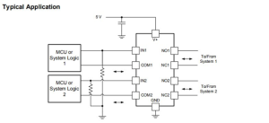
V+ was 5 V in this application, even though it can be any voltage listed in the Recommended Operating Conditions. On the V+ pin, a decoupling capacitor is advised.
IN is, by default, pulled low to GND in this application. Choose the appropriate resistor size depending on the GPIO’s current driving capacity, desired power consumption, and switching frequency. Use pull-up resistors in their place if the GPIO is open-drain.
Any voltage between the recommended operating conditions’ minimum and maximum supply voltage ratings may be used for the power supply. A suitable bypass capacitor should be installed at each VCC terminal to avoid power disturbances. Using a 0.1-F bypass capacitor for devices with a single source is advised. A 0.01-F or 0.022-F capacitor is advised for each VCC pin if there are many pins labeled “VCC,” as the VCC pins will be connected internally.
A 0.1-F bypass capacitor is advised for each supply pin in devices with dual supply pins that operate at different voltages, such as VCC and VDD. It is OK to parallel many bypass capacitors to filter out noise at various frequencies. Capacitors of 0.1-F and 1-F are frequently used in parallel. For best results, the bypass capacitor should be mounted as near as feasible to the power terminal.
Although closely connected to loop antenna theory, reflections and matching are distinct enough to merit separate explanations. A reflection may occur when a PCB trace makes a 90° turn. The trace’s altered breadth mostly causes this. The trace width increases to 1.414 times its breadth at the turn’s apex. This throws off the transmission line’s properties, particularly the trace’s distributed capacitance and self-inductance, which causes the reflection.
All PCB traces must inevitably make turns because they cannot all be straight. The corner-rounding procedures shown in the below figure improve over time. The final one is the only example that keeps the trace width constant and reduces reflections. NO, NC and COM switch I/Os that are not in use can either be left floating or connected to GND. The IN pin, however, must be either driven high or low. Floating control inputs may increase ICC or unknown switch selection states because partial transistor turn-on occurs when control inputs are at threshold levels.
The bidirectional switch, also known as the analog (or PETR) switch, is an electronic element that functions similarly to a relay but doesn’t have any moving parts. A pair of MOSFET transistors, one of which is an N-channel device and the other a P-channel device, typically serve as the switching element. When turned on, the device can conduct analog or digital signals both ways while isolating the switched terminals when turned off. Most analog switches are produced as integrated circuits in packages with numerous switches (typically two, four, or eight). These come from the 4000 series and include the 4016 and 4066.
The gadget’s control input may be a signal that alternates between the positive and negative supply voltages, turning the device on and off according to the voltage’s positive or negative. To turn switches on or off, other circuits are made to talk to a host controller via a serial connection.
The switched signal has to stay inside the boundaries of the positive and negative supply rails, which are attached to the P-MOS and N-MOS body terminals. The switch often offers good isolation between the control signal and the input/output signals. High voltage switching is not done with them.
Thanks for reading. If you thought this post was interesting, feel free to look around the rest of our website for other content similar to what you just read. If you have any questions about the content of this article or any other article that can be found on our website, please feel free to leave them in the comment box below, and we will try our best to respond to them.
Contact us at ICRFQ, your leading electronic distributor of electronic components in china, if you want more information or wish to purchase the TS5A23157. We will ensure that you receive the best product at the best price possible.
WhatsApp us