
Last Updated on October 22, 2023 by Kevin Chen
Chips are the microprocessors, memory, and other electronics that make up the hardware of almost any modern device.
Without them, there would be no smartphones, laptops, tablets, smart speakers, drones, or pretty much any other digital device you can think of.
As the demand for smaller devices continues to increase and manufacturers explore ways to reduce the size of chips while also increasing their functionality and efficiency, integrated circuit packaging has become an essential element of chip manufacturing.
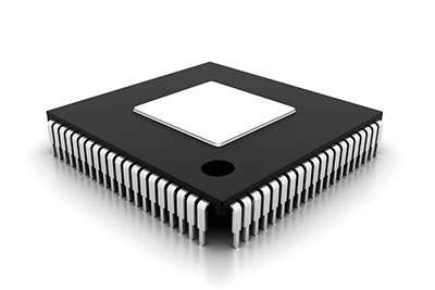
Integrated circuit packaging refers to how an integrated circuit is housed or encased so it can be used for its intended purpose. There are several different ways to package an integrated circuit, with each offering its own set of advantages and disadvantages depending on what you plan on doing with the chip.
In this article, we’ll take a deeper look at what chip packaging is and why it’s so important for making smaller electronic devices. We’ll also cover some common types of chip packaging and all their pros and cons.
Importance of chip packaging
Like many other products, the packaging is the last stage of the manufacturing process. After the chip has been designed and manufactured, it will be packaged and ready to be shipped to the final buyer.
Why is chip packaging essential? Here are the reasons:
Protection
Integrated circuits are quite delicate products. If they were to be packaged in unprotected environments, they would be prone to damage from physical impacts. In other words, if you threw them out of a moving car window, they would most likely break and become unusable.
Other than the physical factors, chips need to be protected from unseen forces. These can be heat, moisture, and dust. These elements can easily affect the functionality of a chip.
Interconnection
Integrated circuits are designed to work with other chips. They can’t function on their own; they need other chips to work. This is why chip packaging is so important. Packaging allows for easy interconnectivity to other chips as well as easier assembly of the product.
Integrated circuits are also used in a variety of products, and they need to be interconnected with each other and the outside world, so packaging allows for this connectivity.
Easy distribution
Packaging also provides an organized distribution system that will make it easier for the end user to get their hands on the product.
Integrated circuits have complex designs that require them to be organized in a certain way, and packaging helps organize these designs so that they can be easily accessed when needed. This makes it easier for end users to get what they want from the product.
Structure of chip package body
The package body is made up of two or more components that are assembled together to form the finished product. The components may be discrete pieces that are simply glued together or they may be formed by etching into a larger piece before assembly.
In either case, they should fit well together with no gaps between them and no sharp edges that could cause damage during handling and soldering operations.
The body usually has an insulation layer on one side (the “back”) so that it can be mounted on a PCB without shorting it. A layer of adhesive may also be applied to hold it in place until final assembly with other parts.
Types of Packaging Chip: Classification of chip packaging
There are various ways in which we can classify chip packages. One way is based on how they are mounted on the circuit board. Under this, we have through-hole mount packages and surface mount packaging.
Through-hole mount packages are those that have leads that are inserted into holes on the circuit board and then soldered to the circuit.
Surface mount packages are those that have leads that come out from the top of the package and are soldered to the circuit board.
In addition, chip packaging can be classified based on how they are formed. Under this classification, we have molded chip packages and multi chip modules.
Multi Chip modules are those where multiple integrated circuits (chips) are packaged together in one package as a single unit. In contrast, molded chip packages are those where only one chip is packaged in a single package.
Molded chip packaging is done by first creating a mold of the integrated circuit using a material such as silicone rubber or epoxy putty, and then injecting molten plastchip into it to form the plastic package housing around it.
The molding material is chosen based on its thermal properties and its ability to flow easily over small bumps and contours of the integrated circuit.
It also needs to be able to withstand high temperatures during soldering processes and not deform easily when exposed to solvents used for cleaning off flux residues left from solder joints.
Otherwise, the most common types of chip packaging include:
-Pin-grade array: In this packaging, the integrated circuit is surrounded by a number of pins or leads. The pins are usually aligned in rows and columns on the underside of the package.
-Quad flat pack: This packaging is in the form of a rectangular parallelepiped. The integrated circuit is placed on a carrier substrate, and the leads are bent to form rows and columns. The rows are connected to the substrate by small bridges or tabs. The quad-flat package is usually used for small chips with high pin counts.
-Dual in-line: This packaging is popular for medium to large chips. It consists of two rows of pins, each row being perpendicular to the other one.
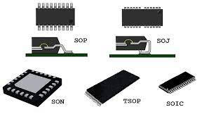
-Small outline: This packaging consists of two rows of pins or leads, with the top row being perpendicular to the bottom one.
-Quad flat no-lead: This type of packaging is commonly used on the surface mount packaging.
-Flip-chip: This packaging is used for mounting the chips on the boards by using solder bumps. The integrated circuit is placed upside down, and the leads are bent to form rows and columns. The rows are connected to the substrate by small bridges or tabs.
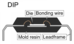
-DIP packages: DIP stands for Dual In-line Package. This is the most commonly used packaging for chips. It consists of rows and columns of pins, which are connected to the substrate by means of a plastic base.
-PQFP packages: The Plastchip Quad Flat Packages are usually used for medium to large chips. They consist of two rows of pins, each row being perpendicular to the other one.
-PFBGA packages: The Plastchip Fine Pitch Ball Grid Array consists of rows and columns of balls placed on top of each other in a square pattern with an interconnect grid between them.
Material for the chip Package
Beyond the type, you should also pay close attention to the material used in the chip packaging. The type of material used may have an electrical and chemical impact on the chip.
Electrical: The electrical properties of the material have a huge impact on the chip. For example, copper has a conductivity of about 2.5×10 S/m, whereas silver has a conductivity of about 3×10 S/m. Therefore, silver is much better for the electrical contact between package and chip (and between package and PCB).
Chemical: This is one of the most important factors in determining the type of material used in packaging. This is done keeping in mind the fact that the packaging and the chip components may come into direct contact and trigger chemical reactions. Therefore, the materials used in packaging should be as inert as possible.
The chemical properties of the material also have an impact on the heat dissipation and thermal characteristics of the package.
Use of substrates
To keep up with the high demand for chip packaging, different substrates or interposers have been widely used. In this context, a substrate is a part of the chip package that specifies the mechanical strength of the board while at the same time connecting the semiconductor with external devchipes.
The package substrate is the most important part of the chip packaging, as it determines the mechanical strength and electronic characteristics chips of the package. It can be a printed circuit board (PCB), a ceramchip or plastchip substrate, or a flexible film.
The substrate may also include metalization layers to improve electrical conductivity. It is usually made from an insulating material such as glass or epoxy resin, with one side having electronic connections and the other side having additional layers for mechanical support.
In many cases, a sheet metal layer is used for mechanical support and to provide some form of protection against potential damage during handling and soldering.
What is die attach material in the chip package?
Die attach material (DAT) is a thin layer of adhesive that is applied to the back side of an integrated circuit die after the semiconductor dies are attached to the package substrate. The bonding material forms a thin film that protects the die and provides mechanical support during handling and handling. DAT is also called a heat-sensitive adhesive (HSA).
DAT has a lower coefficient of thermal expansion (CTE) than solder paste, which results in less thermal expansion mismatch between DAT and the chip package substrate. This helps in maintaining electrical contact between chip and PCB substrate, which improves reliability.
The adhesive used for DAT can be various types such as cyanoacrylate adhesives, epoxy adhesives, polyurethane adhesives, and silicone adhesives. They are usually chosen based on their physical properties such as viscosity, temperature resistance, mechanical resistance, etc., and cost-effectiveness.
The application of HSA depends on its physical properties it can be used for any type of chip packaging 0402 size chip carriers or through-hole packages. Some HSA may have to be cross-linked before use to improve adhesion and mechanical strength against vibration or shock loads during shipment or handling.
Encapsulants in chip package
Another common feature in chip packaging is the use of encapsulants. An encapsulant is a protective material that is added to the surface of an electronic component. Encapsulants are designed for protection against mechanical, chemchipal, and/or electronic damage. It is also used to improve the surface finish of the component as well as prevent contamination from entering the package.
An encapsulant can be applied by dipping, spraying, or using a dispensing system such as a syringe. The type of encapsulant used depends on its properties and application. Some common types of encapsulants are epoxy resin, cyanoacrylate adhesive, and silicone adhesive.
Key properties of encapsulants include:
-Resistance to chemicals and moisture
-Ability to withstand high temperatures
-Ability to withstand mechanical impacts
-Ability to be cured at room temperature
-Chemically inert
Wire bond assembly
This is another aspect of chip packaging that you should know. This is a process in which the component is attached to a conductive layer by soldering. The wire bond assembly is another way to attach the chip to its package. The component needs to be mounted on a printed circuit board (PCB). The PCB is then covered with a thin layer of solder. This forms the connection between the component and the PCB.
Wire bond assembly can be used for different types of components such as memory chips, transistors, and integrated circuits. It is also used in making electrical connections between components inside a computer system as well as connecting external circuits to internal electronic equipment such as communication systems and electronic devices.
The main advantage of wire bond assembly is that it is a quick and easy way to make electrical connections between electronic components. It is also a cost-effective solution as compared to other methodologies.
The main disadvantage of wire bond assembly is that it is susceptible to corrosion which can result in the malfunctioning of the system.
BGA – Ball Grid Array chip package
This type of packaging consists of two flat layers on both sides of the chip and is separated by a ball grid array (BGA). In this type of packaging, the chip will be placed in an area with holes at each corner.
These holes will allow for the BGA wires to enter into the chip through its bottom side or the top side depending on how you look at it. The BGA structure allows for more flexibility while manufacturing and routing than other types.
Conclusion
We have discussed different types of chip packaging and what you should know about them So, next time you buy chips you should know the type of packaging that comes with it. You can use a sourcing agent such as ICRFQ to get details of the packaging type that has been used.
If you want to find more Electronic Components Distributors, please check out the following articles:
Electronic Components Distributors In the USA
Electronic Components Distributors In UK
Electronic Components Distributors In China
Electronic Components Distributors In India
Electronic Components Distributors In Singapore
Electronic Components Distributors In Malaysia
Electronic Components Distributors In Vietnam
Electronic Components Distributors In South Korea
- Where to buy IC chips? The Best Guide? - March 26, 2024
- Breaking Down Barriers: Overcoming Obstacles in Cross-Border Electronic Component Trade - March 4, 2024
- Everything You Need to Know About Amplifier IC Chips - March 4, 2024


