
Last Updated on May 28, 2022 by Kevin Chen
The demand for complicated and small-sized printed circuit boards (PCBs) has increased as the need for sophisticated technology, high speed, high performance, and microdevices has increased. As a result, PCBs have shrunk in size, are available in a variety of configurations, and can be designed to suit specific application needs.
As a result, a wide range of multilayered PCBs is being created. 4-layer PCBs are widely utilized in a variety of applications. These PCBs are used in a variety of electronics and communication devices. Do you want to learn more about them, particularly their stack-up structure and types? What are the advantages they provide, and what are the areas in which they can be used? You’ll get the answers to all of your queries if you read the entire post. But first, what exactly are PCB layers?
PCB Layers Explained
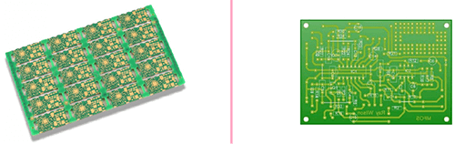
There are many different types of PCB to pick from to meet the needs of your product, including single-sided, multilayer, and even flexible boards. These circuit boards have many layers that contribute to their functioning, making them suitable for various jobs.
It can be challenging to decide when so many options are available, but we’re here to help you grasp the essentials to make an informed decision.
Regardless of which board you choose, it must be built on a solid foundation of several laminated materials.
Substrate Layer
A PCB’s substrate layer is commonly constructed of fiberglass, which provides the board with its rigidity. Most boards will use this material as their substrate except for flexible PCBs manufactured on flexible polymers such as Kapton. Other materials, such as epoxies, can be used as substrate PCB layers, but they lack the longevity that FR4 (found in fiberglass) gives for a high-quality board.
Copper Layer
After that, a thin layer of copper foil is heat fused to the board. When we talk about different layered PCBs, we’re talking about how many copper layers they have. When making a single-sided PCB, one layer of conducting material is utilized on one side of the board, and the opposite side is used to incorporate various electronic components. On the other hand, double-sided PCBs can put conductive copper and components on both sides of the board, rather than just one.
Due to the use of vias to rotate between the top and bottom layers, these double-sided boards enable closer routing traces. The circuits on one side of the board can be connected to the circuits on the other side of the board using holes punched into it, which can be very beneficial in many electrical goods.
The copper layer thickness of your PCB is determined by the amount of power it must resist. PCBs that must manage much power may have a thicker copper layer than others.
Soldermask Layer
The solder mask layer is put in after the copper layer has been applied. This gives the PCB its green color, and it’s employed to isolate the copper layer from any other metal or board parts that can disrupt the copper lines. This layer is particularly significant for the manufacturing process since it aids the user in soldering the components to the correct locations on the board.
Silkscreen Layer
By putting letters, numbers, and symbols on the board, the silkscreen primarily assists us, humans, in better understand the board and the functionality of individual pins or LEDs. The layers listed above are all present in various PCBs and are critical to the board’s functionality.
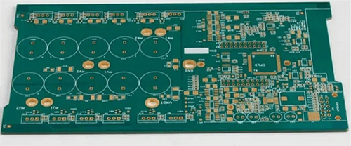
What is a 4 Layer PCB?
The 4-layer printed circuit board (PCB) is the most prevalent of all the multilayered variants. To route electrical signals, a 4-layer PCB’s stack-up is highly sturdy, and it consists of Inner Layer 2, Top Layer, Inner Layer 1, and Bottom Layer. The top and bottom layers are sandwiched between the inner layers (Inner Layers 1 and 2). As a result, a four-layer PCB consists of two signal layers plus a positive voltage layer (VCC layer) and a ground layer, also known as the GND layer, or three signal layers plus a GND layer. More surface space is available for traces in a 4-layer PCB design. As a result, this design structure provides good signal routing for both low and high-speed communications.
The Beauty of 4 Layer PCB
Makers have known about 4 layer PCBs for a long time but have rarely experimented with them. Four-layer boards are now within reach of makers because of the emergence of PCB prototyping facilities worldwide and freely available CAD software. But what exactly are four-layer boards, and how may they benefit your next project?
Makers’ circuit construction techniques have been constrained since their inception. Breadboards allow for the reuse of components, whereas stripboards allow for permanent fixtures. Makers have had access to printed circuit boards, but only in the most basic forms (using the toner transfer method). These circuit boards (particularly double-sided boards) eliminate the need for wires, but they lack features like through-hole plating and silkscreen. On the other hand, new fabrication houses have resulted in low-cost prototyping PCBs (as little as $2 for 5 components).
As a result, maker projects can now include SMD devices, such as QFN and BGA packages, allowing for more sophisticated circuits and smaller designs. But, in addition to double-sided PCBs, 4 layer PCBs are also accessible to makers. Many makers’ designs will suit two-layer boards, prompting the question, “Why would I want to use a four-layer board?”
It’s essential to know the difference between two and four-layer boards to appreciate the advantages of four-layer boards. As the name implies, four-layer boards have four separate copper layers for routing and power, whereas two-layer boards only have two copper layers. As a result, four-layer boards have two more signal routing layers, allowing for lower PCB layouts (as well as the ease of integrating complex devices such as BGA that may have as many as 200 connections).
Makers who want to market their creations can also benefit from four-layer boards. Electronic goods sold commercially must comply with FCC or CE rules, including emissions requirements that require circuits not to release radio energy above a certain threshold. Two-layer PCBs have a hard time controlling emissions, whereas four-layer PCBs can use shielding from power planes and ground planes to absorb emitted energy from traces.
Signals can be routed throughout the PCB stack, and ground planes can be found on the top and bottom levels of four-layer PCBs; however, power and ground are more often found on the two inner layers. The four-layer configuration can help simplify signal routing by removing power and ground connections from the signal routing layers, freeing up space for signals.
Four-layer PCBs do have various disadvantages that make their use challenging. To begin with, four-layer PCBs are more expensive, making them unsuitable for simpler designs. Second, traces in the interior layers of four-layer PCBs might be hidden, making circuit debugging extremely difficult. It would be more practical to rely on the CAD drawings of the designs instead of following traces on the PCB if a circuit required troubleshooting, but this can also be an advantage. Because hidden levels are nearly impossible to observe, using four layers can help dissuade engineers from reverse-engineering your design (only x-rays can be used to see these inner layers).
Four-layer PCBs can help you miniaturize your design while improving EMI performance and allowing for more complicated routing. At the same time, they are pretty sophisticated (because of the low cost of PCB fabrication now available to makers), so it would not be a terrible idea to try them out to see how they can help you with your next project.
Why Are Printed Circuit Boards Layered?
Nearly every modern item we use today has a printed circuit board (PCB). Their main tasks are to connect electronic components electrically and give mechanical support. PCBs are constructed in layers. The material’s structure, durability, conductivity, and organization are provided by these layers built of various materials.
Printed circuit boards often have solder mask layers, silkscreen layers, solder paste layers, mechanical layers, and one or more copper layers, depending on their complexity.
The PCB’s boundaries are contained in the outer layer. Additional mechanical layers may contain tooling specs and other mechanical data.
The routing layers and the ground and power planes are all found in the copper layers.
A solder mask is a solder resist coat applied to the PCB’s external layers to protect them from oxidation and prevent solder bridges from forming between adjacent solder pads. Green is the most popular color for a solder mask, but it is also available in various other colors.
The reference designators for the electronic components on the top and bottom sides of the board, among other things, are found in the silkscreen layers. Permanent non-conductive ink is commonly used to print the text. The most common color for silkscreen is white, but other colors are also available.
The SMD pads’ position, size, and shape on the board are all contained inside the solder paste layers. The apertures in the SMT stencil are then made with this information.
The Benefits of Using Multiple Layers on Printed Circuit Boards
Miniaturization
Designers can use multilayer PCBs to reduce the size of their boards by layering them. This is critical as the industry continues to be driven by the shrinking of electrical devices.
Reduced Complexity
Multiple layers simplify PCB routing by allowing copper traces from one layer to connect to traces from other layers to complete the path.
Supply and Ground Isolation
Supply and ground layers are separate on multilayer PCBs (4 or more layers). This prevents short circuits by isolating the supply and ground pins.
Simplify Construction & Reduce Weight
Reduce or eliminate the need for connectors on multiple separate PCBs.
Higher Density of Assembly
Single Layer Vs. Multiple Layer Printed Circuit Boards.
Electronic components are on one side of a single layer PCB, while the conductor pattern is on the other. Electronic components can be placed on the top, bottom, or both sides of multilayer PCBs, with one or more conductor designs.
Simple electronics often employ single-layer or single-sided PCBs. They are inexpensive to produce and are commonly found in high-volume applications such as calculators, radios, and printers.
For somewhat advanced technology, such as HVAC systems, power supplies, LED lighting, and vehicle dashboard lighting, double-layer boards are required.
Medical equipment, Complex data storage, GPS technology, and satellites are all explored on multilayered boards.
Difference between 2 Layer PCBs and 4 Layer PCBs
Stack-up Differences
Only a two-sided trace, comprising a bottom and an identical top layer, exists on a double-layered motherboard. The four-layer motherboards, on the other hand, have four layers. These four layers may have the same structure as the two-layer board, but they are all laminated together with a layer of fiberglass.
Design Differences
In terms of design, a two-layer motherboard has nearly double the surface area of a single-layer PCB design. Double-layer motherboards allow for connections between identical surfaces, allowing for a massive electrical cross-connection, thus doubling the surface area.
However, keep in mind that this is a fraction of the surface area of a four-layer printed circuit board. The resin-impregnated layer used to join the four layers aids in the creation of connection patterns between them, quadrupling the performance surface area.
Functionality Differences
A two-layer motherboard with two similar layers on opposite sides makes connecting the different electrical components easier. This also eliminates connection latency, resulting in higher performance levels.
As a result, while four-layer motherboards may have a few operational delays, having two additional layers implies they will perform better in the long run than two-layered boards.
Making of Prototype Differences
A four-layer circuit board prototype may be more challenging to construct than a double-layered one due to the additional layers. It’s essential to recognize that software solutions can assist relieve the stress that comes with prototyping.
The use of automated software speeds up the prototype creation process. Automated programs like azure, Gerber, Adobe XD, and others have built-in standards that help speed up the circuit board creation process.
Cost Differences
Compared to the two-layer PCB design, the four-layer PCB design is more complex and vulnerable to prototype creation. As a result, a four-layer motherboard will eventually be more expensive to produce than a double-layered one.
It is critical to realize that you do not have to take on the difficult task alone of creating a printed circuit board. Outsourcing this part of your project to a professional prototyping service provider, such as PCBA Store, may be good. It will not only provide you with a well-crafted prototype, but it will also enable you to save money.
Conclusion
PCBs are used in all electronics and devices we use daily. PCBs can be produced from a single layer or a multilayer pool. As a PCB designer, you’re bound to have many questions about the various layers, designs, and applications. We hope that this post has solved all of your PCB layers questions.
For more details on PCB and other electrical components, contact us at ICRFQ. We manufacture the best electrical components in the whole of China.
If you want to find more Electronic Components Distributors, please check out the following articles:
Electronic Components Distributors In the USA
Electronic Components Distributors In UK
Electronic Components Distributors In China
Electronic Components Distributors In India
Electronic Components Distributors In Singapore
Electronic Components Distributors In Malaysia
Electronic Components Distributors In Vietnam
Electronic Components Distributors In South Korea
- Where to buy IC chips? The Best Guide? - March 26, 2024
- Breaking Down Barriers: Overcoming Obstacles in Cross-Border Electronic Component Trade - March 4, 2024
- Everything You Need to Know About Amplifier IC Chips - March 4, 2024


