
Last Updated on October 22, 2023 by Kevin Chen
Multilayer PCBs have become quite popular in various industries throughout the years. Multilayer PCBs, such as 4-layer PCBs, 6-layer PCBs, and so on, are readily available today. PCBs with six layers have become commonplace in small wearable devices and other mission-critical communication equipment. What is it that makes them so popular? What distinguishes them from different types of multilayer PCBs? This article aims to provide you with all of your information regarding 6 layers PCB manufacturers.
What is a PCB Layer?
The signal transmitting vertical levels to the board’s plane makes up a PCB layer. A two-layer board, for example, has top and bottom layers, but a four-layer PCB has a top, inner 1, inner 2, and bottom layer.
Every PCB layer has an insulating substrate in the middle (Fire Retardant Version4). This substrate is Teflon-based epoxy-saturated fibreglass.
Solder masks are commonly seen on the surface copper layers of typical PCBs. The mask can appear in both the upper and lower levels at times. These masks are put to the board layers as a liquid or sheets.
What is the 6 Layer PCB Board?
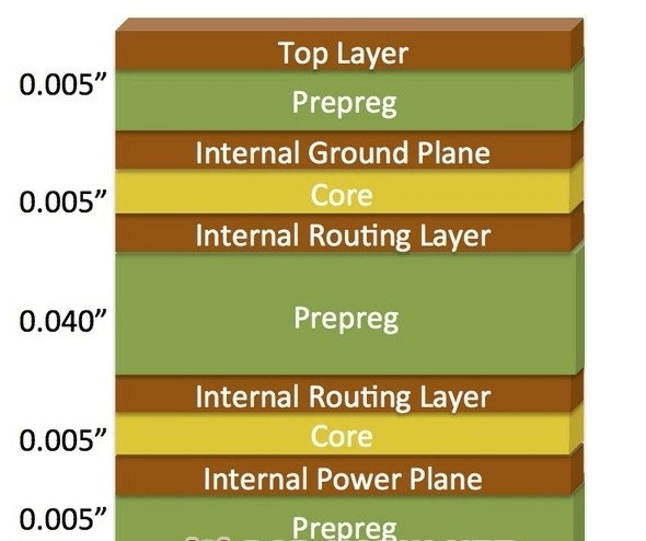
Six layers of circuit board material make up a six-layer PCB. It’s a four-layer PCB with two signal layers interspersed between the planes. Two internal planes, two internal layers, two external layers, one layer for the ground, and one layer for the power make up a six-layer stack.
Using a 6-layer stack reduces EMI between layers and enables fine-pitch components with a high net count. This style of PCB reduces EMI while also allowing for more high- and low-speed signal routing. High-speed signals are routed through the two internal layers, while low-speed signals are routed through the two external layers.
Although an 8-layer or 4-layer stack-up may be better appropriate for a particular application, PCB designers prefer a 6-layer stack-up. Engineers and designers can use a conventional 6-layer PCB to assist them in balancing the need for efficient manufacturing procedures with signal integrity issues.
The Importance of a 6-Layer Board Stack-up in PCB Design
For decades, multilayer printed circuit boards have been a standard in the design industry. Electronic components have dropped in size, allowing more circuitry to be built onto a single board. As a result, new PCB design and manufacturing technologies have been necessary to accommodate them. The 6-layer board stack up was once only a means to get more traces onto the board than a 2- or 4-layer board could handle. To maximize the performance of the circuitry, it is now more vital than ever to construct the proper layer layout in a 6-layer stack up.
Due to poor signal performance, a PCB layer stack-up that is not designed correctly will be subject to electromagnetic interference (EMI). A well-designed 6-layer stack up, on the other hand, can eliminate difficulties caused by impedance and crosstalk while also improving the circuit board’s performance and durability. A solid layer stack-up setup will also aid in protecting your data.
Factors that Determine the Designs of a 6-layer PCB Stack-up
Several elements influence the design of a 6-layer PCB stack-up. A conventional 6-layer PCB will aid in suppressing EMI and use various types of RF equipment. Any errors made during the stack-up design process will impact the PCB’s performance. As a result, there are a few things to think about as you go through the design process.
Area Of Application
A six-layer PCB can serve a variety of purposes in various sectors. As a result, determining the application or industry before beginning the design process is critical.
Design Configurations
You’ll need to figure out how to construct the PCB 6-layer stack. You can choose from a variety of 6-layer PCB stack-up options. The needs of your application determine these settings.
Electrical Specifications
It’s critical to evaluate how much current the 6-layer PCB is carrying at any given time—this aid in providing the necessary signal lines and routes for the current to take.
Cost Of Designing And Production
The cost of constructing the 6-layer PCB stack-up must be factored in. The cost of creating a 6-layer PCB stack uprises as the design becomes more sophisticated.
Electrical Specifications
Because this stack-up is employed in applications with varying temperature requirements, you must look into every aspect of thermal identification and specification while creating a 6-layer PCB stack up.
Component Density
Because it helps to provide varied electrical connections, it’s necessary to think about the types and quantity of components put on a 6-layer PCB stack up.
What is the Best 6-Layer Stack-up Configuration?
The stack-up configuration you choose for your 6-layer board will be heavily influenced by the goals you want to achieve with your project. If you have many signals to route, you’ll need four signal layers. If the signal integrity of high-speed circuits is a top issue, you’ll want to go with the one that provides the best protection. The following are some of the different configurations found in 6-layer boards.
The initial stack up setup that I first started working with many years ago is the first layer stack up option:
- Top Signal
- Inner Signal
- Ground Plane
- Power Plane
- Inner Signal
- Bottom Signal
Because the signal layers are not shielded, and two of the signal layers are not close to a plane, this is probably the worst design you can utilize. This design was mostly abandoned as signal integrity and performance requirements became essential. You may restore a nice 6-layer stack by replacing the top and bottom signal layers with a ground plane. The downside is that signal routing is limited to only two internal layers.
The inner signal routing layers are placed in the middle of the stack up, which is the most widely used 6-layer layout in PCB design:
- Top Signal
- Ground Plane
- Inner Signal
- Inner Signal
- Power Plane
- Bottom Signal
The planes are arranged so that the inner signal routing layers, which are often utilized for higher frequency transmissions, are more shielded. This stack-up can be improved by using a thicker dielectric material to increase the distance between the two inner signal layers. The disadvantage of this arrangement is that it reduces the overall capacitance of the power and ground planes by separating them. This will necessitate the incorporation of greater decoupling into the design.
The 6-layer stack-up configured to provide the best signal integrity and performance is not widely used. To add a ground layer, the signal layers are reduced to three:
- Top Signal
- Ground Plane
- Inner Signal
- Power Plane
- Ground Plane
- Bottom Signal
This stack immediately upsets each signal layer for optimum return path characteristics near a ground plane. Planner capacitance is also created by placing the power and ground planes near one other. However, the downside is that you lose one signal layer for routing.
A few things are to consider when designing 6-layer PCB stack-ups for various applications.
A 6 layers PCB manufacturer’s stack-up can help you achieve higher performance by suppressing EMI, allowing you to employ various types of RF devices, and including multiple fine-pitch components. Any errors in the stack-up design will have a significant negative impact on the PCB’s performance. What should I do first? Here’s how to make the best stack-up decision possible.
- It’s critical to assess and address the number of grounds, power, and signal planes your PCB may require as a first step toward stack-up design.
- Ground planes are vital for any stack-up because they insulate your PCB better. They also reduce the requirement for external shielding cans.
For varied applications, here are a few tried and true 6-layer PCB stack-up designs
For Denser Boards with A Small Footprint
If you want to route a denser board with a small footprint, you can go with four signal planes, one ground plane, and a power plane.
For Denser Boards Combining Wireless and Analog Signals
The internal and external signal layers are separated by two enclosed ground planes in this sort of stack-up. This stack-up architecture prevents EMI from interfering with internal signal layers. The stack architecture is also perfect for RF devices because the alternating power and ground planes give excellent decoupling.
For Printed Circuits with Sensitive Traces
If you want to make printed circuit boards with many sensitive traces, you should go with the following stack-up: signal layer/power layer/2 signal layers/ground/signal layers. Sensitive traces will be well-protected, thanks to the stack. The stack is designed for circuits that use high-frequency analog or digital signals. The low-speed communications on the outer layer will get insulated from these signals. The inside layer provides this shielding while allowing signals with varied frequencies or switching speeds to be routed.
For Boards That Will Be Used Close to A Powerful Source Of Radiation
The ground/signal layer/power/ground/ground/signal layer/ground stack-up will be ideal for this type of board. EMI can be effectively suppressed by using this stack-up. This stack-up is also appropriate for circuit boards used in a loud setting.
Benefits of Using 6 Layer PCBs
Because of their designs, six-layer PCBs are becoming more common in modern electronic circuits. These circuit boards are popular among electronic makers because of the following benefits.
Small Footprint
These printed circuit boards are smaller than others due to their multi-layered architecture. This is particularly useful for little devices.
Quality-driven Designs
As previously stated, a 6-layer PCB stack-up design necessitates extensive preparation; this aids in the reduction of errors in their detailing, resulting in high-quality construction. Furthermore, all major PCB manufacturers today use a variety of testing and inspection processes to guarantee that these circuit boards are suitable.
Lightweight Construction
Lightweight components are being used to create compact PCBs, which helps lower the overall weight of a PCB. The 6-layer circuit boards, unlike single or double-layered PCBs, do not require several connectors to interconnect components.
Improved Durability
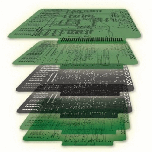
Multiple insulation layers between circuits are used on these PCBs, as shown in the diagram above, and these layers are connected utilizing protective materials and various prepreg bonding chemicals. This increases the PCBs’ long-term resilience.
Excellent Electrical Properties
These printed circuit boards have exceptional electrical qualities, allowing for incredible speed and capacity in small packages.
Whether you are a seasoned OEM or a first-time electronic maker, you will need a high-quality 6-layer PCB manufacturer for your projects. Knowing their importance in your gadgets, getting them from a reputable provider like Twisted Traces is critical. For many years, the company has provided its clients with high-quality 6-layer printed circuit boards and multilayer printed circuit boards. The company has designed circuit boards for micro smart gadgets, military equipment, and healthcare equipment.
Applications of the 6-Layer PCB Stack up
Depending on the structure and arrangement of the stack up, it can be utilized in various applications. You should be aware that each stack up has its unique arrangement that meets the needs of a variety of applications.
Some of the applications for which a 6-layer PCB stack-up can be used are listed below:
● Machines to be developed by the processing industry
● Industry of aviation
● The manufacturing of medical equipment is a part of the medical sector.
● For the manufacture of cell phones, there is a communication industry.
● The automotive industry is responsible for the production of various parts for automobiles.
Frequently Asked Questions about printed circuit board.
● In PCB design, what is the significance of a 6-layer PCB stack up?
A 6-layer PCB stack-up can maximize performance by developing superior layer designs. Impedance and crosstalk issues can also be avoided with this stack-up.
How can I keep a 6-layer PCB stack from overheating?
Overheating can be reduced by employing measures such as using thermal dissipation equipment and appropriately aligning the stack up to improve heat flow.
Conclusion
Due to the multiple advantages, a 6-layer PCB stack-up is an excellent choice for various applications. The electrical and mechanical qualities of this stack-up are excellent. You’ll require a high-quality 6-layer PCB builder whether you’re a beginner or experienced in electronic production. As a result, it’s critical to have your facts straight.
Lastly, at ICRFQ, we are the best manufacturers of electrical components in China. Please contact us today if you need to purchase PCB layers or any other electrical components.
If you want to find more PCB Electronic Components Distributors, please check out the following articles:
Electronic Components Distributors In the USA
Electronic Components Distributors In UK
Electronic Components Distributors In China
Electronic Components Distributors In India
Electronic Components Distributors In Singapore
Electronic Components Distributors In Malaysia
Electronic Components Distributors In Vietnam
Electronic Components Distributors In South Korea
- Where to buy IC chips? The Best Guide? - March 26, 2024
- Breaking Down Barriers: Overcoming Obstacles in Cross-Border Electronic Component Trade - March 4, 2024
- Everything You Need to Know About Amplifier IC Chips - March 4, 2024


