
Last Updated on October 24, 2023 by Kevin Chen
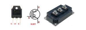
Image source Leets Academy
In today’s fast-paced digital world, IGBT tends to serve the switches. This type of transistor has evolved to be a very important power electronic component that is highly demanded in most application areas.
The transistor is used in both the switching and power amplification applications.
You will find insulated gate bipolar transistors in both domestic and industrial applications.
It is called insulated because it’s a thin layer of oxide provides the electric insulation on the gate against the semiconductor layers.
The ‘bipolar’ name is derived from the fact that it is a three-terminal transistor with the n-p-n configuration. The P layer is sandwiched between the two n-type layers.
These transistors tend to feature even in the most sensitive applications where other transistors don’t seem to perform well.
What makes IGBTs so special?
Before you even know the unique features that are packed in the insulated gate bipolar transistors, it will be prudent to know how they work, or their basic working mechanism.
Construction, structure and configuration of the IGBT

Image source electronics Notes
If you are aware of MOSFETs. If so, then you should have an idea of the design and structure of the IGBT. They have the same structure. Just like MOSFE, IGBT is also a three-terminal transistor. This means that it has conductor terminal at the middle and and oxide layer that separates the metal gate from the semiconductor.
The key feature that separates IGBT from MOSFET is its p layer is right in the middle of the two n layers. This arrangement is quote similar to that of the BJT.
In short, the structure of the IGBT ensures that it utilizes the best features of both MOSFET and BJT.
In the real sense, IGBT comprises of four semiconductor layers which end up forming the PNPN structure. It has a heavily doped n+ emitter layer, a slightly doped n- base layer, a p+ buffer layer and another n- layer which serves as a drift layer.
The collector C is connected to the P layer and at the same time the emitter E is located between the P and the N layers. Take note of the presence of the P substrate in the IGBT construction.
When it comes to the IGBT configuration, there are various options that you can use depending on the application area.
You can configure the IGBT to work as a high-side switch or you can make it function as a low-side switch.
In a high-side switch configuration, you will connect the collector terminal to the positive terminal of the power source. This means that the load will be positioned between the E terminal and the ground. A positive voltage is applied at the gate terminal which will also serve as a reference voltage for the emitter.
When in the low-side configuration, the emitter terminal of the transistor is connected to the ground. Here the load will be between the collector and the positive power source.
Remember that the high-side and the low-side configurations are used when the IGBT is used as a switch.
The other two common configurations for IGBT include the half bridge and full bridge configurations.. The half-bridge is when you connect two IGBTs in series. Full-bridge configuration refers to when you connect four IGBTs in parallel.
In overall, the structure and configuration options of the insulated gate bipolar transistors is among the key reason for their versatility. This means that the transistor can be used for different purposes and in different application areas.
IGBT working principle
As I have already mentioned, the working mechanism of IGBT is based on the operation of two types of transistors; MOSFET and BJT (bipolar junction transistor). Once you understand how the two work, you will be able to deduce the full operation of the insulated gate bipolar junction transistor.
The working mechanism of IGBT is based on the biasing of the Gate-Emitter terminals and at the same time on the Collector-Emitter terminals.
From the discussion about the configurations, the Collector-Emitter terminal is connected to the positive voltage source (Vcc).
- It all starts by applying positive voltage across the gate terminal of the transistor. When this happens, an electric field will be created at the gate terminal and will attract the electrons which will move towards the gate oxide and the n-type drift region.
- An increase of electric current will expand the width of the channel hence allowing more electrons to flow from the positive voltage source to the drain region. This results in a process known as channel modulation and the IGBT will be turned on.
- When the IGBT is on, it will fully allow unlimited electric current to flow from the collector terminal to the emitter terminal. This will subsequently forward-bias the p-n junction that is based at n-type drift section of the transistor.
- The free flow of current through the base region of the transistor will allow both the holes and electrons to move towards the n-type drift region. This will eventually improve the electric conductivity in this region hence current will flow towards the target load or electric device.
- The operation will continue until the IGBT reaches a certain threshold as designated by the circuit requirement and the load. At this stage, the IGBT will switch off hence stopping the flow of current.
- Now, lets say the IGBT is switched off. This means that the voltage at the gate terminal will be zero and there will be no flow of electrons between the source and the drain. At this state, the IGBT will work in the reverse-bias mode.In this state, the reverse voltage will be at the p-n junction mainly due to the load. If this voltage is not well regulated it can lead to a serious failure of the IGBT. To avoid this, special circuits are integrated with IGBT to prevent incidences of spike voltage generated by the inductive load.
Comparing IGBTs vs other transistors
Just to give you a glimpse of how effective insulated gate bipolar transistors are, the table below gives a full comparison between these related transistors
| Transistor characteristic | BJT | MOSFET | IGBT |
| Transistor voltage rating | High but less than 1kV | High but less than 1kV | Very high and more than 1kV |
| Current rating | Less than 500A | Lower than 2A | Higher than 500A |
| Input Parameter | Base Current | Voltage Vgs | Voltage Vge |
| Input Drive Power | High | Low | Low |
| Switching speed | Low | medium | High |
| Switching Loss | Low | Fast | Low |
| Cost | Low | Medium | High |
| Input impedance | Low | High | High |
Advantages of IGBT
Based on the features and working mechanism of IGBT, you can tell easily outline the reasons behind their popularity. Let’s look at the top advantages of these insulated gate bipolar transistors.
- Simple technology: From the working principle that we have just discussed, everything about IGBT transistor is straightforward. Starting from the way it allows current to the load and the manner in which it switches off the circuit. It is capable of executing fast switching speed using simple technology. This also makes the transistor easy to use and integrate in circuits.
- High voltage and current capacities: From the comparison table above, it is clear that insulated gate bipolar transistor has high current and voltage capabilities. This explains why it is suitable for voltage applications such as electric vehicles. Similalrly, the transistor can be used for low voltage applications.
- Fast switching speed: This is the main advantage of the IGBT. It can inverse the flow of current within a short time. It is faster than both MOSFET and BJT.
- High reliability: The reliability of the IGBT is based on the fact that it can perform well in different conditions. High temperatures rarely affect the operation of IGBT.
- Premium safety: IGBTs come with built-in safety features that protect it from the dangers of current and voltage surge. Such features go a long way in extending the service life of these transistors.
- IGBTs have low drive power: When compared to the alternatives such as BJTs and MOSFETs, IGBTs have a way lower drive power. This means that they only require a small amount of current to trigger an action. This feature ensures that is the main reason why IGBTs are known for proper usage of electric energy.
What are the constraints of IGBT
Despite the advantages, there are some cons that are associated with using IGBTs
The most common problem with of IGBT is the high switching loss. This can end up affecting both the performance and effectiveness of the transistor.
Another major problem is the cost. Compared to other transistors such as BJT, IGBT are slightly more expensive. Currently the is a global shortage of IGBT in the market and this is also affecting their price.
Buy IGBTs in China
After knowing how insulated gate bipolar transistors work, the next step is to buy the right one.
If you are in the business of electronics, you would want to buy IGBTs in bulk for sale. This is also ideal if you are buying transistors for projects.
Choosing a reputable IGBT supplier in China is the key to ensuring that you get the right transistor that will serve its purpose.
If you want to find more Electronic Components Distributors, please check out the following articles:
Electronic Components Distributors In the USA
Electronic Components Distributors In UK
Electronic Components Distributors In China
Electronic Components Distributors In India
Electronic Components Distributors In Singapore
Electronic Components Distributors In Malaysia
Electronic Components Distributors In Vietnam
Electronic Components Distributors In South Korea
- Where to buy IC chips? The Best Guide? - March 26, 2024
- Breaking Down Barriers: Overcoming Obstacles in Cross-Border Electronic Component Trade - March 4, 2024
- Everything You Need to Know About Amplifier IC Chips - March 4, 2024


