
Last Updated on October 27, 2023 by Kevin Chen
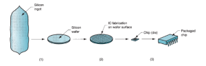
Image Source: FreeImages
Making an IC is a process that involves precise patterning and etching of layers. Looking at the complexity involved, it’s no surprise that it is widely acknowledged as one of the most difficult tasks in the entire semiconductor process.
For decades, IC fabrication has been a major bottleneck for chip makers. It’s a time-consuming, resource-intensive process that requires multiple stages of photolithography and multiple etching processes to cut out the various layers within an IC design.
And all these factors have led to soaring production costs, forcing semiconductor firms to outsource their fabrication needs to third-party contract manufacturers with expertise in this field.
In this guide, we are going to look at everything that entails IC fabrication.
Definition of IC fabrication
Fabrication of an integrated circuit involves finalizing the design on an integrated circuit, placing the design onto a silicon wafer, and then transferring the design to the wafer by means of various techniques.
Step 1: Preparation of wafer
A silicon wafer is the base material for IC fabrication. It is made from a single crystal of silicon. Basically, a silicon ingot is sliced into very thin wafers using a machine called a saw. Briefly, the ingot is fed into a rotating machine where a rotating saw blade slices it horizontally into thin wafers. The saw can produce wafers of different sizes depending on the design of the machine. Once the wafers are sliced, they are loaded into a chemical solution where they remain for several hours. This process is called annealing and it helps to remove impurities and defects from the surface of the wafer.
Step 2: Oxidation
Oxidation is a chemical reaction that involves the formation of an oxide layer on the surface of a material.
Oxides are formed by the combination of oxygen with another element or compound. There are many uses of oxidation in the process of making silicon integrated circuits. For example, oxidation is used to form the insulating layer for the interconnection.
Here, silicon dioxide is formed by exposing the silicon surface to oxygen at high temperature.
Oxidation is also used to form the silicon dioxide surface layer on silicon wafers used for the fabrication of silicon integrated circuits.
Step 3: Diffusion
Next, impurities are diffused into the wafer’s surface to create n- and p-type regions. During this process, the wafer is placed in a vacuum chamber and heated to high temperatures.
During these high-temperature operations, the silicon wafer is bombarded with ions to create n- and p-type regions in its surface.
In the case of n-type regions, a gas containing hydrogen is used to create an excess of electrons on the silicon surface. For p-type regions, the gas contains an impurity such as boron to create an excess of positive holes in the silicon surface.
Step 4: Ion implantation
It is followed by the ion implantation process to introduce impurities. These impurities will act as atoms when the silicon is heated again to form the silicon dioxide layers. During ion implantation, ions are accelerated towards the silicon wafer using an electromagnetic field. There will be a silicon wafer in a vacuum chamber. The ions that are accelerated will collide with the silicon wafer and are embedded inside it.
Step 5: Chemical Vapor Deposition
A chemical vapor deposition (CVD) chamber is used for the formation of silicon dioxide layers. The silicon wafer is placed inside a CVD chamber and heated to a high temperature.
The silicon wafer is initially kept at a low temperature to allow a silicon vapor to form. The silicon vapor will react with oxygen to form silicon dioxide. CVD is a process in which chemical reactions are used to produce materials. Usually, CVD is done at low pressure. This helps to produce a silicon dioxide layer on the silicon wafer.
Step 6: Photolithography
Photolithography is the next step in IC fabrication. It is the process of transferring a pattern printed on a photoresist layer to the silicon wafer.
During photolithography, a silicon wafer contains a layer of photoresist and a thin layer of silicon dioxide.
After the silicon dioxide layer is formed, the photoresist layer is applied on top of it. Then, a photomask is placed above the photoresist layer.
A beam of light is projected from behind the photomask. This causes the photoresist layer to be exposed to light and its shape is transferred to the silicon dioxide layer.
Step 7: Ultraviolet light exposure
The silicon wafer is exposed to ultraviolet light. When the silicon dioxide layer is exposed to ultraviolet light, it becomes very reactive and starts to form silicon. This is called a chemical reaction. This reaction causes the silicon dioxide layer to be converted into silicon. This process exposes the pattern transferred during photolithography and creates a silicon layer where the silicon dioxide layer used to be.
Step 8: Metallization
This refers to the process of coating a metal layer on a surface. The surface either be metallic or non-metallic. The metal layer provides a conductive path on the silicon wafer. Metal such as copper, aluminum ,or gold can be used as the metal layer.
They react with carbon atoms in the silicon wafer and form a thin nickel layer. The silicon wafer is placed in an electrolytic solution containing metal ions and copper ions. The copper ions are released from the solution and travel through the electrolytic solution to reach the silicon wafer. There, they react with the nickel ions to form a copper layer.
Step 9: Packaging
This is the final step of IC fabrication. After everything has been done, the silicon wafer needs to be packaged in readiness for sale. A number of IC packaging options exist, but the ones used most commonly for logic devices are plastic dual in-line packages (PDIP), small outline J-leaded packages (SOJ), and thin small outline packages (TSOP). They are all made of plastic.
The final IC package is mounted on a printed circuit board (PCB), which has many other components on it. The PCB is then connected to the outside world via a cable or a socket, or sometimes directly soldered onto a circuit board.
Epoxy resin and plastic are also used to seal the packaged IC chip. This is done to prevent dust and other unwanted particles from getting into the chip.
Key factors to consider before IC fabrication
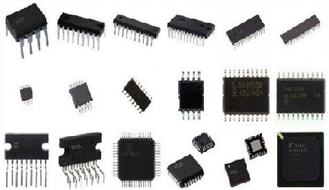
Image source Eprocus
When you design a chip, there are a few key factors that you must consider before you can move on to IC fabrication.
These can include the complexity of the chip design, the choice of materials, and of course the type of process that you plan to use.
The complexity of the chip design
– First of all, you must understand the complexity of the design. If you are fabricating a simple chip, it is likely that you can do this in-house. However, if the design is more complicated, you might want to outsource this to a third-party manufacturer. In some cases, a combination of these two methods might be the best approach. Choosing the materials
– Next, you must choose the right materials for the chip. This is an important consideration that will have a significant impact on the cost of the entire process. The type of process that you use
– Finally, you must choose the type of process for fabricating the chip. This will depend on the complexity of the design, the materials that have been selected, and the time and resources that are available.
Companies that are in charge of IC fabrication usually lay down the requirement specifications for the fabrication process. From there, they proceed to execute the complete fabrication of the integrated circuit.
These specifications are usually written based on the target use of the IC. For example, the fabricator should know the exact application area for the IC before they proceed with the fabrication.
Who does the fabrication of the IC?
Outsourcing is a common practice in the business world today.
Whether it is outsourced engineering or other business functions, it is a practice that has grown significantly in recent years. In the semiconductor industry, IC fabrication has long been outsourced to third-party manufacturers.
In fact, the majority of semiconductor firms choose to outsource their fabrication needs to third-party contractors that are experts in the field.
Traditionally, fabrication of ICs has been done in centralized fabs located in low-cost countries.
This is because the capital-intensive process requires large-scale production facilities, which are usually too expensive to set up in developed countries.
However, things are changing in the industry. In fact, fabless semiconductor companies are now exploring the option of regional fabs, which are located closer to their place of operation.
Although these facilities are not as large as centralized fabs, they are still large enough for the fabrication requirements of most advanced semiconductor firms.
What is the cost of IC fabrication
The price of IC fabrication depends on the complexity of the design, the materials used, and the fabrication process.
In general, complex designs with multiple layers have a higher price than simpler designs with fewer layers.
Similarly, the use of exotic materials like GaN and BiCMOS increases the price of fabrication. Fabrication cost is also determined by the duration of the process. There are two ways to reduce the cost of IC fabrication — reduce the complexity of the design and use cheaper materials.
Always keep in mind that a high-quality fabrication will get the price tag that it deserves.
How to maximize accuracy of IC fabrication
Accuracy is one of the most important parameters in IC fabrication.
It is a measure of how close your fabricated product is to what you intended it to be. It is important that you maximize accuracy while fabricating your ICs because any deviation at this stage can lead to a poor quality product that may not work as expected.
There are a few ways that you can maximize accuracy while fabricating your ICs.
The most important thing is to understand what can cause inaccuracy while fabricating your ICs.
You can then take steps to reduce the chances of this happening by taking the necessary precautions.
Slip-ups during fabrication are usually caused by human error. So, it is important that you take all precautions to ensure that there is no mistake. You can do this by keeping your work area clean and tidy.
You can also keep a check on the machines that you are using for fabrication. Machines are prone to breaking down, which can lead to mistakes.
So, it is important that you keep them well-maintained to reduce the chances of a mistake and errors.
The good news is modern technology has led to the development of various equipment that can accurately fabricate integrated circuits.
Also, big-name distributors in China are quite selective when it comes to the IC fabricators that they choose. For example, ICRFQ source our ics from reputable IC fabricators who are known for their quality and accuracy.
Choose a reputable IC distributor in China
Choosing the right IC distributor in China can be challenging. However, if you follow the tips outlined in this blog, you’ll be well on your way to making a good choice.
Here’s a quick summary of the tips:
– Understand your needs and objectives – Before you begin an IC sourcing process, it is important to understand your needs and objectives. Only then will you be able to determine what type of supplier you’re looking for.
– Do your research – The next logical step is to do your research. It is important to visit the Chinese market and find potential distributors for your product. Make sure you visit different distributors so as to have a clear picture of the options available.
– Shortlist potential distributors – After visiting several distributors, shortlist the potential distributors. This can be done by comparing the different aspects of each distributor. You can also talk to reference customers of each distributor to gain a better insight into their services and offerings.
– Negotiate with distributors – After shortlisting, it is important to negotiate with distributors. During this process, make sure you’re clear about your product specifications and requirements. It is also recommended to get a signed contract from your distributor before making a payment.
Once you follow all these tips, you will eventually end up with the right distributors of IC.
If you want to find more Electronic Components Distributors, please check out the following articles:
Electronic Components Distributors In the USA
Electronic Components Distributors In UK
Electronic Components Distributors In China
Electronic Components Distributors In India
Electronic Components Distributors In Singapore
Electronic Components Distributors In Malaysia
Electronic Components Distributors In Vietnam
Electronic Components Distributors In South Korea
- Where to buy IC chips? The Best Guide? - March 26, 2024
- Breaking Down Barriers: Overcoming Obstacles in Cross-Border Electronic Component Trade - March 4, 2024
- Everything You Need to Know About Amplifier IC Chips - March 4, 2024


