
Last Updated on April 10, 2022 by Kevin Chen
In electronic devices, transistors are the most common component. Bipolar Junction Transistor (BJT) and Field Effect Transistor (FET) are the two most common varieties of transistors (FET). NPN and PNP transistors are two different types of BJTs based on their construction. We’ll talk about the differences between the two transistors in this article, so take a deep breath and prepare yourself because we’re about to dive right in.
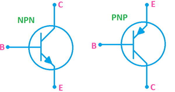
Definition of PNP Transistor
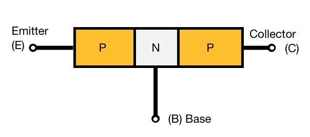
Two p-type blocks and one n-type block make up the PNP transistor. Emitter, base, and collector are its three terminals. PNP transistors have a p-type base and an n-type emitter and collector.
PNP’s emitter-base junction is forward biased, while the collector-base junction is reverse biased. The majority charge carrier is pushed toward the base by the emitter-base junction, resulting in the emitter current. The p-type material’s hole mixes with the n-type material to form the base current. The leftover hole is captured by the collector and reaches beyond the negatively biased collector-base area, causing collector current to form. As a result, the collector circuit carries the entire emitter current.
Making of PNP Transistor
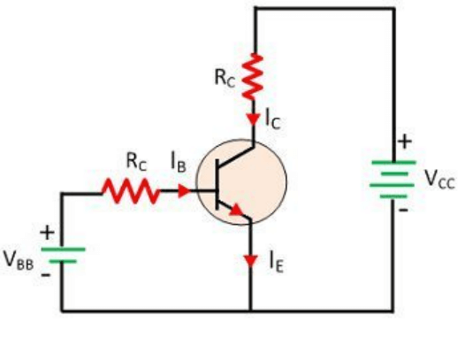
PNP and NPN transistors have identical characteristics, with the exception that the voltage and current biasing directions are reversed for any of the three possible configurations: common base (CB), common emitter (CE), and common collector (CC) (CC), Because the base terminal of a PNP transistor is always biased negative concerning the emitter. The voltage between the base and emitter terminals VBE is negative at the base and positive at the emitter terminal. The emitter voltage is also positive compared to the collector voltage (VCE).
The voltage sources are coupled to a PNP transistor, as depicted in the diagram. The RL connects the emitter to the VCC, limiting the maximum current that can flow through the device connected to the collector terminal. The base voltage VB is coupled to the emitter-biased base resistor RB. In a PNP transistor, the base terminal must be approximately 0.7volts more negative than the emitter terminal to cause the base current to flow.
The appropriate biasing of the transistor junctions is the key distinction between a PNP and a PN transistor; the current and voltage polarities are always opposite.
Basics of P-N-P
Between the p-types of p-n-p transistors, there is an n-type. In this transistor, holes make up most of the carriers responsible for the current generation. The working procedure is identical to the n-p-n method. In terms of polarity, however, the applications of voltages and currents differ.
PNP Transistor Applications
If you’re learning about these components for the first time, industrial sensors can throw a wrench in your knowledge if you’re not careful. PNP and NPN sensors are supplied with positive and negative power lines, respectively, and then output a signal to indicate an “on” state. During an “on” state, PNP sensors produce a positive signal to your industrial controls input, whereas NPN sensors produce a negative sign. It would be simple to believe that a PNP transistor is controlled by positive voltage if you learned to utilize sensors before learning about transistors.
Of fact, things aren’t quite so simple, as the PNP and NPN sensor designations refer to the type of transistor (or equivalent for more complicated devices—some can even be wired in either configuration) utilized within. The base signal is the perceived stimulus, and the positive collector output of a PNP sensor—which is most typical in this type of application—is then coupled to a PLC input signal. When turned on, NPN or “sinking” output sensors act opposite, sinking ground voltage to an input. The control engineer never sees the base switching voltage (+ for NPN and − for PNP), making these concepts incomprehensible from a fundamental standpoint.
Definition of NPN Transistor
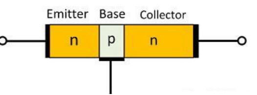
The NPN transistor is a bipolar junction transistor in which the first letter N represents a negatively charged material layer and the second letter P represents a positively charged layer. A positive layer sits between two negative layers in these transistors. NPN transistors are commonly employed in circuits to switch and amplify electrical signals.
The transistor is connected to the circuit board by three terminals: base, collector, and emitter. When current travels through an NPN transistor, the transistor’s base terminal receives the electrical signal. The collector generates a greater electric current than the one passing through the base, and the emitter transfers this stronger current to the rest of the circuit. Current passes from the collector to the emitter in this transistor.
This transistor is commonly used due to its ease of manufacture. To function correctly, an NPN transistor must be made of a semiconductor material that can carry some electric current but not as much as more conductive materials like metal. Silicon is one of the most widely used semiconductors, and NPN transistors are the simplest silicon transistors to produce.
A computer circuit board uses an NPN transistor. A computer’s contents must be translated to binary code, which is accomplished by a series of little switches that turn on and off circuit boards. For these switches, NPN transistors can be employed. A strong electric signal turns the switch on, and the lack of a signal turns it off.
Making of NPN Transistor
An NPN transistor has a positive base voltage and a negative emitter potential. The base terminal is always positive to the emitter terminal, and the collector supply voltage is positive. Through the load resistor RL, the collector of an NPN transistor is connected to the VCC. This load resistor limits the current that flows through the maximum base current.
NPN Transistor Applications
While both PNP and NPN sensors perform the same basic function, you may be wondering why one is preferred over the other. Some distinctions exist, and NPN transistors are favored in most circuit design applications. This is because the “N” substrate can transport electrons far quicker than the “P” substrate can transport positive electron holes. This provides a significant benefit in high-speed switching and amplifier circuits. NPN transistors are also more accessible and cheaper than PNP transistors, which adds to their advantage.
On the other hand, specific circuits benefit from PNP-type transistors and would be difficult, if not impossible, to build without them. A class B amplifier, for example, uses a matched pair of PNP and NPN transistors to amplify oscillating signals efficiently. This second type of switching option is quite beneficial when building a circuit.
Difference Between NPN and PNP Transistor
Bipolar Junction transistors are three-terminal devices composed of doped materials commonly utilized in amplification and switching applications. In essence, every BJT has a couple of PN junction diodes. When two diodes are connected, a sandwich is formed, with one semiconductor sandwiched between the other two types. As a result, there are only two varieties of bipolar sandwich, namely PNP and NPN. In semiconductors, the electron mobility of NPNs is often higher than the whole mobility. As a result, it can handle a significant quantity of current quickly. Furthermore, the fabrication of this transistor from silicon is simple.
- Both PNP and NPN transistors are made of various materials, and their current flows are likewise varied.
- Two layers of P material are sandwiched between two layers of N material in PNP transistors. Two layers of N material are sandwiched between two layers of P material in NPN transistors.
- A positive voltage is applied to the collector terminal of an NPN transistor to cause current to flow from the collector to the emitter. A positive voltage is applied to the emitter terminal of a PNP transistor to generate current flow from the emitter to the collector.
- When you boost the current to the base terminal of an NPN transistor, it switches on and conducts entirely from the collector to the emitter. When the current to the base terminal is reduced, the transistor turns ON less and less until it no longer conducts across the collector to emitter and shuts off.
- The working concept of a PNP transistor is that when a current is present at the transistor’s base terminal, the transistor turns off. When there is no current at the PNP transistor’s base terminal, the transistor turns ON.
The distinction between NPN and PNP transistors, utilized in many electrical and electronic projects, is discussed here.
Conclusion
While NPN transistors are more frequent as essential components for the reasons stated previously, the PNP paradigm has found a home in the industrial control realm for at least two reasons. First, while NPN sensors may make the most sense to someone with an electrical engineering degree, PNP sensors—which have a positive output and signal an “on” state—can be more approachable to technicians and engineers from other fields. Another reason is that if an NPN sensor’s output wire frayed and became grounded, a controller would perceive it as an “on” signal, which could be dangerous in particular conditions.
In industry, NPN sensors are used, and they are more common in Asian manufacturing than in Europe and North America. While one kind of control may be more appropriate most of the time, having both NPN and PNP alternatives provides you with a certain bit of control versatility.
Lastly, for any electrical component purchase, contact us at ICRFQ, we are the best electrical components manufacturers in China.
If you want to find more Electronic Components Distributors, please check out the following articles:
Electronic Components Distributors In the USA
Electronic Components Distributors In UK
Electronic Components Distributors In China
Electronic Components Distributors In India
Electronic Components Distributors In Singapore
Electronic Components Distributors In Malaysia
Electronic Components Distributors In Vietnam
Electronic Components Distributors In South Korea
- Where to buy IC chips? The Best Guide? - March 26, 2024
- Breaking Down Barriers: Overcoming Obstacles in Cross-Border Electronic Component Trade - March 4, 2024
- Everything You Need to Know About Amplifier IC Chips - March 4, 2024


