
Last Updated on October 22, 2023 by Kevin Chen
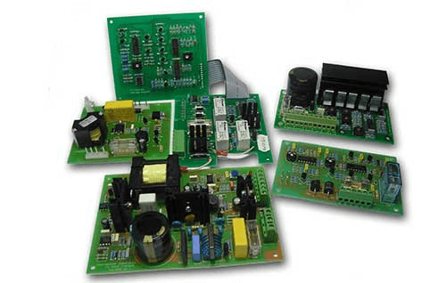
Image Source: Flickr
In the manufacturing industry, manufacturers are constantly challenged by new technologies and techniques that enable faster production and more efficient processes.
This is particularly true in the creation of printed circuit boards (PCBs) for electronic devices. The ability to reverse engineer printed circuit boards has become increasingly important as manufacturers seek to make their production processes more streamlined, cost-effective, and automated.
PCBs are multi-layer printed circuit boards used in electronics to house electronic components or an electronic device. To understand what a PCB is and its various uses, you need a little background on how it’s made.
In this article, we will provide you with a comprehensive guide to PCB reverse engineering with detailed explanations of the process and why it’s so important in the world of electronics from hobbyists to professionals.
What is PCB Reverse Engineering?
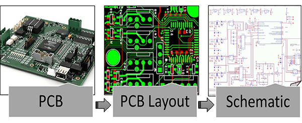
PCB Reverse Engineering is the process of taking an existing printed circuit board (PCB) and creating a digital copy of it. The digital copy can then be used to create new printed circuit boards (PCBs) or lay out a printed circuit board design on a computer-aided design (CAD) tool.
In reverse engineering, engineers and technical experts do not create the PCB from scratch. Instead, they use various tools and techniques to extract information about the PCB and its design. There are a number of ways that manufacturers can extract design data from a PCB.
These include image analysis, data decapping, and chip extraction. Each of these methods involves removing the components from the PCB and then using a process to understand how they’re connected to one another.
Image analysis involves taking an image of the PCB and then analyzing the image to determine the components that are present on the PCB. With data decapping, engineers remove the integrated circuit (IC) chip from the PCB and then use a device to read the data stored on the chip.
Chip extraction involves removing the components from the PCB and then measuring the size, shape, and pitch of the components.
History of PCB reverse engineering
As the PCB manufacturing process has evolved, PCB reverse engineering has evolved alongside it. The PCB manufacturing process has gone through three main phases: manual assembly, semi-automatic assembly, and full automation. These phases have corresponded with a corresponding increase in PCB reverse engineering.
Manual assembly was the most common method of manufacturing PCBs before the early 1980s. At this time and before, PCBs were manufactured in a completely manual process. The design of the PCB was done on paper, and the board was manufactured using a photolithography process.
However, this process created several problems, including the fact that the PCBs were expensive to produce and had a high defect rate. As a result, the semiconductor industry’s growth created a need for a better way to produce PCBs.
In response to this need, a few manufacturers began developing new PCB manufacturing equipment to address these issues. This new equipment allowed manufacturers to produce PCB boards more efficiently, economically, and with a lower defect rate. A Brief History of PCB Reverse Engineering
Reasons Why is PCB Reverse Engineering Important?
While PCB reverse engineering is not a new process, it is still an important process. The practice of reverse engineering PCBs has become even more important as technology continues to advance and evolve.
Over the years, the PCB manufacturing process has evolved significantly. It has gone from being a manual process to an automated process. It has also gone from being an expensive process to being one that is more cost-effective.
The advantages of automated PCB manufacturing include a lower defect rate, faster production time, and the ability to produce PCBs with a smaller design.
However, PCB manufacturers must protect their designs from competitors. If a competitor reverse engineers a PCB design and copies that design, the competitor can produce PCBs with the same design, thereby infringing on the manufacturer’s design.
Overview of the PCB Reverse Engineering Process
In order to reverse engineer a PCB design, you must first understand how a PCB is manufactured. PCBs are usually manufactured with a multi-layer printed circuit board (PCB).
To create a PCB, manufacturers begin by designing the PCB on a computer CAD program. The CAD program then creates a layout for the PCB. After the layout is complete, the manufacturer uses the layout to cut the PCB from a sheet of the copper-clad printed circuit board (CC- PCB).
The manufacturer then applies a thin layer of copper to both sides of the PCB. This process is often referred to as copper plating. The PCB manufacturer uses a photoresist process to create the design on the copper PCB. The photoresist process uses a chemical to remove copper from the copper PCB board.
The manufacturer uses the layout to create a stencil for the PCB’s design. The stencil is made of a thin material that will be used to apply ink to the PCB. The manufacturer uses the stencil to apply the ink to the PCB.
Key Steps in the PCB Reverse Engineering Process
There are various steps that are followed in executing the PCB reverse engineering. Thes steps include;
-Data collection and analysis
-Drawing, scanning, and photography
-Uploading the image to a relevant program
-Construction of a 3D PCB layout
-Creation of schematics
-Testing of the PCB
We are going to look at each of these steps and what happens in each one of them.
Step 1: Data collection
Like in any other project, data is of great importance. This data is used to create a complete design of the PCB. The data includes the following;
-Detailed information about the PCB that is required for reverse engineering
-The details of the components that are used on the PCB
-The details about how each of these components is mounted on the PCB
-The details about how each circuit works.
The data also includes any information that is required to create a schematic from it. This data can be obtained from many sources such as manufacturers, suppliers, and employees who have worked with this product in some way or another.
Step 2: Drawing, scanning, and photography
It is called reverse engineering because there is an existing PCB. You will use it to develop your PCB. So, the process is set off by drawing the PCB on a sheet of paper. It is scanned using a scanner and then digitized using an image editor. The images are then stored in a file that is made up of layers.
You can also use a high-quality camera to take photo of the PCB. But, the board is scanned first and then digitized.
Step 3: Upload the image
Once you have taken the picture, drawn or scanned the image of the PCB, you can now upload it to the website.
This will help you in getting your PCB design.
However, you have to upload the image of the PCB in a correct format like PDF, DXF or SVG.
The image must be clear and identifiable and the resolution should be high enough so that it can be printed out. There should not be any defects on the PCB. The color of the PCB should also be accurate so that it can be scanned accurately.
Step 4: Construct the PCB layout
You will now use your image to construct the 3D PCB layout.
You can use a 3D PCB layout software to help you in creating the PCB.
This is the stage where you will design your PCB and test it.
The software will have many features such as schematic, netlist, and layout.
You can select the components that you want to include in your PCB. The software can even print out the circuit diagram for you on a piece of paper.
You can also save your design as an image file and print it out using a printer or can also save it on a USB drive and take it along with you while traveling.
There are various tools in this step that make up the task easier for you.
For example, there are different types of drill patterns that are available to use with your design. You will be able to choose from them depending on how much space is available in your case or how much room you have for routing the wires on your PCB design.
Basically, the steps followed for constructing the PCB layout include;
-Painting the holes;
-Routing the wires;
-Placing the components;
-Determining the PCB size; and
-Creating a top board for your PCB.
-Cleaning the tracks and creating a test board
-Marking the holes
-Creating the board outline
-Cutting the traces and vias on your PCB
Step 5: Create schematics
A schematic is a circuit diagram and is used in PCB design to show the circuit arrangement of all the components on your PCB. The schematic needs to be created in order to show what should be done and when it should be done. For example, if you want to create a custom PCB for a project, you will need to create a schematic for that project. The schematic is used as a guide for creating your PCB design.
Step 6: Create Gerber files
Gerber files are used in the manufacturing process of your PCB and are sent along with your order. You can use them as an electronic signature or can also use them as documentation of your completed board design.
This step involves creating two files; one is the Gerber file and another is the BOM (Bill of materials).
The Gerber file contains information about how the components are connected together on your PCB along with the drill pattern for drilling out each hole on your PCB using an appropriate drill bit, drill size, etc.
The BOM contains information about all the components that are required along with their quantity, price, and delivery terms (if any).
There is also another type of file which is referred to as ‘BOM’ but it has less information than BOM files or even only includes one part number and its quantity and delivery terms (if any). This type of file has no relation whatsoever to BOM files mentioned above in Step 6 except for its name itself which was derived.
Step 7: Testing the PCB
Once you have created the gerber files, you need to test the PCB for any mistakes or errors.
You can use one of the many available PCB layout software to test your board.
In addition to testing your board, you also need to check whether there are any other errors during the manufacturing process which might have caused a problem with your design. For example, if you created a faulty component or a mistake in routing the traces on your PCB then that might show up during testing.
If there are no errors during testing then it is time to assemble your PCBs and ship them out!
Method of PCB Reverse Engineering
Other than the above-listed steps, it is imperative to note that PCB reverse engineering is divided into two main types. These are destructive PCB RE and Non-destructive PCB RE. What is the difference between them? Well, the main difference is that in destructive PCB RE, the PCB is dismantled while in Non-destructive PCB RE, the PCB is tested first and then dismantled if there are errors.
The following steps are followed in destructive PCB reverse engineering:
Step 1: Identify all components on the board.
Step 2: Remove all components from their sockets using a Dremel tool and make notes of which sockets have which types of components attached to them.
Step 3: Identify all traces and routes on the board.
Step 4: Remove all traces and routes from the board using a Dremel tool and make notes of which traces and routes have which type of trace or route on them.
Step 5: Identify all pads on the board.
Pads are located at the bottom side of the PCB, between traces, or at the top side of PCB between vias (the connection points between traces). Pads are used to connect external devices with ICs or other components in a circuit board.
Pads can be identified by their shape, location, and size. The following image indicates how pads are identified on a PCB:
Step 6: Identify all vias on the board.
Vias are used to connect traces and routes together in a circuit board. Vias can be identified by their shape, location, and size. The following image indicates how vias are identified on a PCB:
Step 7: Identify all components on the board.
This step is optional, depending on the type of circuit board being used and the components to be removed.
X-ray computed tomography
This is another technique used for PCB reverse engineering. This method is used to detect the presence of components on the PCB. This method is done by using an X-ray machine and a special camera. The process starts by placing a PCB on the X-ray machine. Then, you will need to place a special mask over the PCB that has holes in it. Next, you will need to place your components on the PCB and then place another mask over them so they can be imaged clearly through the X-ray machine.
Multilayer film emulation
In this technique, the film is placed on the PCB, and a special camera will be used to image the film. The image of the film can then be used to determine what type of material is used in the circuit board.
Electron beam inspection
This technique uses an electron beam to scan a PCB. The electron beam will then create a pattern on the PCB. This pattern can then be used to determine what type of material is used in the board.
Fourier transform infrared spectroscopy
This technique uses a special instrument called Fourier transform infrared spectrometer (FTIR) to detect the presence of components on the PCB. The FTIR is able to identify different materials used in the circuit board, such as resistors and capacitors.
Limitations of PCB reverse engineering
While PCB reverse engineering is a useful process, it does have some limitations. For example, the data decapping process can often compromise the quality of the data that is extracted from the PCB. As a result, the data of a PCB might not be accurate after it has been decapped.
Another limitation of PCB reverse engineering is that it is an expensive process. Conducting reverse engineering on a PCB will cost several thousand dollars. Additionally, there is no guarantee that the process will be successful.
The schematic created during the PCB reverse engineering process might not be accurate. The schematic might not accurately reflect the connections between the components on the PCB.
Precautions to take during PCB reverse engineering
Here are some precautions that should be taken when attempting to reverse engineer a PCB.
– Ensure that the PCB is clean and free of dust, oily residue, and other contaminants.
– Ensure that the PCB is mounted on a board stand. This prevents the PCB from bending or twisting during the reverse engineering process.
– Ensure that you have all of the necessary tools for the reverse engineering process. These tools include a multimeter, DMM, and oscilloscope.
– Ensure that you do not damage any components when removing them from their sockets. You should always handle components carefully to prevent damage or breakage during removal.
– Ensure that you are familiar with how to use all of your tools before starting to reverse engineer a PCB.
When not to Use PCB Reverse engineering
If you don’t have a PCB or if you have a PCB but don’t know what it does or what it’s for, then you would not be able to do reverse engineering on it.
So, you can only do PCB reverse engineering on a PCB that you have or that you know what it’s for. PCB reverse engineering is not recommended if the PCB is old and obsolete.
In such cases, it is best to purchase a new PCB or use a PCB that is newer and more advanced. You should also not use PCB reverse engineering if you don’t have the original parts. This means that the PCB manufacturer might have used some non-original parts.
Getting PCB Reverse Engineering Services
If you don’t have the skills or tools to conduct PCB reverse engineering on your own boards, you can outsource the process.
There are many PCB reverse engineering services available on the market today. To find PCB reverse engineering services, you can do an online search for PCB reverse engineering companies near you.
You can also use an online PCB procurement tool to find companies that can provide PCB reverse engineering services. When you’re conducting PCB reverse engineering, you should be aware that the process is not fully accurate.
In fact, the process can be very imprecise. As a result, it’s important that you understand that the data you get from the PCB might not be accurate.
How do I choose a PCB reverse engineering company?
You should consider the following when choosing a PCB reverse engineering service:
Capabilities. A good PCB reverse engineering company should have the necessary skills and tools to reverse engineer your boards. You should also check the company’s record of previous work.
Cost. You should also consider how much it will cost you to get a PCB reverse engineering service. It’s important that you do not select a company that charges too much for its services if you don’t have enough money to pay for them.
Reputation. When selecting a PCB reverse engineering service, you should check the reputation of the company. There are many online forums and blogs where people discuss their experiences with different companies and share tips on how to choose the best one for your needs. You can also ask other people who have used different services in order to get their opinions on which companies provide quality services at fair prices.
How do I know that the PCB reverse engineering service I have chosen is capable of reverse engineering my board?
You can check the company’s website to see if it offers the required skills and tools to reverse engineer your board. If it does, you should also ask for a sample of previous work.
You should also check whether the company has experience in designing similar boards.
The surest way is to use a sourcing agent such as ICRFQ. We can link you to the companies that offer PCB reverse engineering services, as well as their contact details and their price ranges.
If you want to find more Electronic Components Distributors, please check out the following articles:
Electronic Components Distributors In the USA
Electronic Components Distributors In UK
Electronic Components Distributors In China
Electronic Components Distributors In India
Electronic Components Distributors In Singapore
Electronic Components Distributors In Malaysia
Electronic Components Distributors In Vietnam
Electronic Components Distributors In South Korea
- Where to buy IC chips? The Best Guide? - March 26, 2024
- Breaking Down Barriers: Overcoming Obstacles in Cross-Border Electronic Component Trade - March 4, 2024
- Everything You Need to Know About Amplifier IC Chips - March 4, 2024


