
Last Updated on October 22, 2023 by Kevin Chen
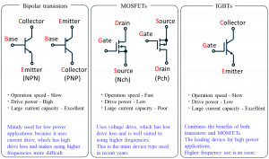
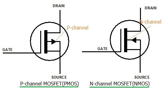
MOSFETs are divided into two categories: NMOS and PMS. The main distinction between NMOS and PMOS is that NMOS uses n-type semiconductors for the source and drain terminals, whereas PMOS uses p-type semiconductors for the Source and drain terminal. This article describes the essential distinction between NMOS and PMOS MOSFET
What is NMOS?
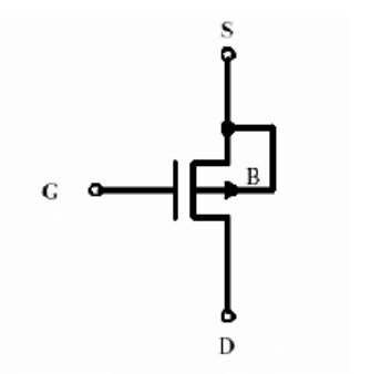
NMOS (NMOSFET) is a MOSFET type, as previously described. The n-type Source and drain, as well as a p-type substrate, make up an NMOS transistor. The holes in the body (p-type substrate) are forced away from the Gate when a voltage is applied. This permits an n-type channel to be formed between the Source and the drain, with electrons carrying a current from the Source to the drain via an induced n-type channel.
NMOS logic is used to describe logic gates and other digital devices that use NMOSs. Cut-off, triode, and saturation are the three modes of operation in an NMOS. NMOS logic is simple to design and produce. However, when the circuit is idling, circuits with NMOS logic gates dissipate static power because DC Current passes through the logic gate when the output is low.
What is PMOS?
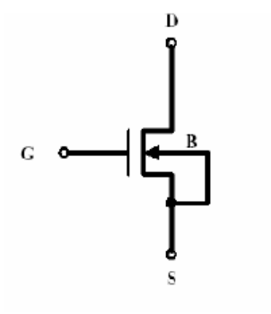
PMOS (PMOSFET) is a kind of MOSFET, as previously stated. A PMOS transistor has an n-type substrate and p-type Source and drain. When a positive voltage is placed between the Source and the Gate (and a negative voltage between the Gate and the Source), a p-type channel with opposing polarities is formed between the Source and the drain.
Through an induced p-type channel, holes carry a current from the Source to the drain. A PMOS will not conduct if the gate voltage is too high, but if the gate voltage is too low. PMOS logic is used to describe logic gates and other digital devices that use PMOS. PMOS is a low-cost technology with strong noise immunity.
PMOS vs NMOS: What’s The Difference?
MOSFETs are divided into two types: NMOS and PMOS. The construction differs: NMOS employs N-type doped semiconductors as the Source and drains, with P-type as the substrate, whereas PMOS does the opposite.
This has several ramifications for transistor functionality. The drain current direction and voltage polarity are the most obvious: the threshold voltage VTH, the VGS, and the VDS are all negative. Second, most carriers in NMOS and PMOS are not the same: NMOS employs electrons while PMOS uses holes. This has a significant impact on the K constant, resulting in a number of differences:
- NMOS transistors are faster than PMOS transistors;
- NMOS transistors have roughly half the ON resistance of PMOS transistors;
- PMOS transistors are less susceptible to noise;
- NMOS transistors have a smaller footprint than PMOS transistors for the same output current;
The NMOS is more commonly employed due to its advantages; however, many applications require the PMOS’s polarization characteristics. NMOS and PMOS are also commonly employed in analog and digital microelectronics. One of the most common MOS structures, in particular, uses both: the CMOS (complementary MOS).
When the voltage VG is low, the NMOS is off and the PMOS is on, resulting in a low impedance path from the output to VCC; when VG is high, the NMOS is on and the PMOS is off, resulting in a low impedance path to ground. This ensures that the output pin is constantly connected to a predictable and stable voltage, which is crucial in digital systems. NMOS and PMOS should, of course, be designed to work in a symmetrical manner.
The Body-Effect
Although the Gate, Drain, and Source characterize the transistor’s operation, the MOSFET is essentially a four-pin device. The fourth port, known as the body, is attached to the transistor’s substrate. The transistor will suffer from the body effect if the voltage between the body and the Source is not zero. The body effect alters the threshold voltage VT and can be utilized to adjust the transistor’s properties dynamically. However, it is usually undesirable when the body node is not directly linked to the source voltage. Every calculation in this article assumes VBS = 0 V, which eliminates the body effect.
Construction and Physical Operation
Silicon wafers serve as the foundation for MOS transistors. This method employs layer-by-layer semiconductor doping and oxide growth to produce N-type, P-type, and insulating areas. Photolithography and chemical etching are used to create geometric shapes. Below is a simplified representation of the NMOS and PMOS cross-sections.
N-dopants (NMOS) or P-dopants (PMOS) are heavily doped in the drain and source regions, while the substrate is doped with the opposite type (N-type for PMOS and P-type for NMOS). This alternation causes a depletion region, which prevents any current from flowing between the drain and the Source, explaining the cut-off region.
The Gate is attached to a thin silicon dioxide layer that acts as a barrier between the Gate and the substrate. The electric field pulls minority carriers to the region below the SiO2 layer when voltage is supplied to the Gate. The MOSFET’s “FET” (Field-Effect Transistor) component. When there is enough charge in that region, the minority carriers become the majority carriers, forming a channel of the same type as the Drain and Source.
The threshold voltage VTH is the gate-to-source voltage resulting in channel inversion. Positive voltages (to attract electrons) and negative voltages (to attract holes) are required for channel construction in NMOS and PMOS, respectively.
The channel has ohmic resistance for a fixed VGS (linear operation mode) as long as VDS is less than VGS – VTH. The charge concentration at the drain is nulled after that, and the channel is “pinched.” A channel pinch-off marks the boundary between the saturated and linear zones. The pinch point moves as VDS grows, and the effective length of the channel decreases, resulting in the previously mentioned channel-length modulation effect.
NMOS and PMOS Applications
Because NMOS and PMOS can be utilized as active loads, voltage-controlled resistors, trans-impedance amplifiers, current reflectors, and even capacitors and diodes, it isn’t easy to cover all of their applications. As a result, we’ll concentrate on the two most common applications: voltage amplifiers and switches. However, the same logic can be extended to other situations.
Amplifier
Because both NMOS and PMOS are “voltage to current” converters, a voltage amplifier can be created by simply adding a resistive load to the current output. On the other hand, the drain current must be independent of the drain voltage to function as a suitable current source (in other words, the output impedance should be high).
As a result, the MOSFET must operate in the saturation region to be used as a voltage amplifier. In addition, because the current equations are very non-linear, the input signal should be kept minimal to avoid non-linear effects. Techniques for circuit linearization can be found in the literature.
MOSFET amplifiers are divided into common-source, common-drain, and common-gate. The role of each pin is what distinguishes them.
Common-Source
The Gate is utilized as an input for amplification, the Source is coupled to a fixed voltage, and the drain is connected to a resistive load. High gains and high input impedance are the most general applications for the common Source. However, the gain is negative, and the miller-effect limits the circuit’s frequency.
Common-Gate
The Gate is coupled to a fixed voltage, and the Source is used as an input. Because the signal is connected to the Source, the input impedance of this amplifier is negligible. It does, however, eliminate the miller effect, resulting in increased bandwidth. Furthermore, there is again. It’s commonly utilized for current-to-voltage conversion in high-frequency applications.
Common-Drain
This amplifier employs the Gate and the Source as output and links the drain to a fixed voltage. This design is commonly employed in buffers because it gives a stable and linear voltage unit gain.
Switch
A good switch has two characteristics: it has a very big impedance and a very small impedance when turned on. Leakage currents will pass through if it fails to open the circuit, and the signal path will become uncontrollable. If it does not close, the signal will be weakened, and power losses will grow.
MOSFETS excels at both qualities, offering wide impedance channels in the cut-off region and low series resistance in the linear area. The command signal is segregated from the signal path, greatly simplifying the control circuit. Low resistance and high gate impedance are desirable in switched-mode power converters because they considerably boost efficiency. Furthermore, the compact footprint of MOS switches greatly increases the density of logic ports on a single chip, which was critical for the digital revolution in modern technology.
Depending on the control signal and current direction, switches can be made from NMOS and PMOS transistors. In microelectronics applications where MOSFET dimensions can be changed, it is critical to design the transistor to have a very low resistance point in the closed state, which can be accomplished by changing the W and L the technology.
In addition, parasitic capacitances should be kept to a minimum to avoid crosstalk through the transistor when it is in the open state. Peak voltage, charge injection, maximum current, and switching time are just a few characteristics that need to be monitored. When using discrete MOSFETs, as most switched-mode power converters do, the transistor switch should be chosen, considering all of the criteria mentioned above and heat dissipation and gate driving. MOSFET switches come in a variety of topologies.
Frequently Asked Questions
PMOS vs. NMOS: which is faster?
NMOS is thought to be faster than PMOS because the carriers in NMOS, which are electrons, travel twice as quickly as the carriers in PMOS, which are holes. However, PMOS devices are more noise resistant than NMOS devices.
What does it mean for an NMOS to be saturated?
Characteristics of Saturation • VDD is connected to the input and Gate. • The gate-source voltage (VGS) is substantially higher than the threshold voltage (VTH). • The MOSFET is switched on (saturation region) • VDS = 0V • Max Drain current flows (ID = VDD / RL) (ideal saturation)
What exactly is an NMOS inverter?
The inverter with a p-device pull-up or a load with a permanently grounded gate. The input signal is used to drive an n-device pull-down or driver. NMOS technology, which is equal to using a depletion load, is dubbed ‘Pseudo-NMOS.’ A variety of CMOS logic circuits use this circuit.
PMOS or NMOS: which is better?
Because of their smaller junction surfaces, NMOS circuits are faster than PMOS circuits. An n-channel junction can have lower capacitance since the operating speed of a MOS IC is mostly restricted by internal RC time constants. The capacitance of a diode is directly proportional to its size. As a result, its speed improves.
Why is PMOS always connected to VDD?
It’s tied to Ground for this reason. The logical choice is to connect the Source to the Ground because the voltage between the Ground and the Source in the NMOS transistor must be positive. The Source is connected to VDD in PMOS because the voltage between the Gate and the Source must be negative.
Why is NMOS a bad passer of 1?
Because the drain in an NMOS receives the higher voltage, the drain in our example is connected to VDD, and the source becomes the output node. Any extra voltage at Vs. would turn the NMOS off, and thus, you would never get a Strong 1 (i.e., VDD) at the output. Thus, NMOS passes Weak 1 (VDD – Vth).
Conclusion
A FET (Field Effect Transistor) is a voltage-controlled device with the ability to modify its current carrying capacity by applying an electric field. Metal Oxide Semiconductor FETs are a typical form of FET (MOSFET).
In integrated circuits and high-speed switching applications, MOSFETs are frequently used. MOSFETs apply a voltage to the oxide-insulated gate electrode to create a conducting channel between the source and drain contacts. Depending on the kind of carriers flowing through the channel, MOSFETs are classified as NMOSFET (commonly known as NMOS) or PMOSFET (often known as PMOS).
For more details, contact us at ICRFQ, we are well versed with PMOS and NMOS. Lastly, we are known to be the best manufacturer of electrical components in China.
If you want to find more Electronic Components Distributors, please check out the following articles:
Electronic Components Distributors In the USA
Electronic Components Distributors In UK
Electronic Components Distributors In China
Electronic Components Distributors In India
Electronic Components Distributors In Singapore
Electronic Components Distributors In Malaysia
Electronic Components Distributors In Vietnam
Electronic Components Distributors In South Korea
- Where to buy IC chips? The Best Guide? - March 26, 2024
- Breaking Down Barriers: Overcoming Obstacles in Cross-Border Electronic Component Trade - March 4, 2024
- Everything You Need to Know About Amplifier IC Chips - March 4, 2024


