Last Updated on October 22, 2023 by Kevin Chen
Image source JavaPoint
For most modern electronic devices, there is always a need to strike a balance between power and energy efficiency. End users always want powerful devices that deliver desirable results while at the same time using less energy which will reduce the running cost of the device.
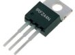
This is where the Insulated Gate Bipolar Transistors (IGBT) come in. They have gained quite a massive popularity in recent years thanks to their energy efficiency and power.
Are you planning to integrate insulated gate bipolar transistors into your devices? Here is a perfect guide for you. We are going to give you a detailed understanding of this transistor. At the end of it, you will be in a perfect place to make a sound decision when buying one.
What is an Insulated Gate Bipolar Transistor?
Insulated Gate Bipolar Transistor (IGBT) is categorized as a three-terminal power semiconductor transistor that is designed to combine desirable electronic properties of bipolar junction transistors (BJT) and MOSFET to operate as a powerful and the most efficient switch. Insulated Gate Bipolar Transistor takes the input characteristics of the MOSFET (known for its high put impedance) and the output characteristics of the MOSFET.
This bipolar transistor has a fast-switching speed, a feature that makes it applicable for high-power applications. It is also used in many other modern applications such as renewable energy applications, and power electronics among others.
IGBT is packed with a plethora of advantages that you should know. But, before you buy one, it will be wise to know about its capabilities and limitations.
Structure and construction of IGBT
An insulated Gate Bipolar Transistor comprises of four layers which end up forming a PNPN structure.
Similarly, it is a three-terminal device that has the Gate (G) Collector ( C ), and Emitter(E). The Gate is the input terminal of the transistor while the emitter and the collector serve as the output terminals.
The collector terminal is embedded to the P layer of the BJT. On the other hand, the emitter terminal is embedded between the P and N layers. The N- layer ends up forming the PN junction J1 of this power transistor.
At the top of the N- layer are two P layers which eventually form the PN junction which will be J2.
The design of the P region is such that it leaves an electric path for the input electrodes coming through the gate terminal. On the other hand, the N+ tend to spread all over the P region.
In terms of the IGBT stricture, the emitter, and the gate serve as the electrodes. The emitter is connected to the N positive region of the transistor while the hate features a silicon dioxide layer insulation.
The base region is usually referred to as an injector layer because it injects holes into the N- region (drift region). The thickness of this drift region is directly proportional to the supply voltage.
In overall, the structure of IGBT is similar to that of power MOSFET when you view it from the vertical dimension. The only difference is that in place of the P-positive collector is the N-positive drain. The result is a vertical PNP junction.
The working mechanism of IGBT
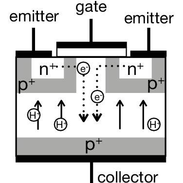
Image source Researchgate
How does an Insulated Gate Bipolar Transistor work?
Now that you know the basic structure and construction of IGBT, it is easy to tell how it works.
From the structure, the Collector (C) and the Emitter (E) terminals are used as current conductors. The Gate (G) serves as the controller. So, the working principle of the IGBT depends on the biasing of the Collector-Emitter terminals and at the same time the Gate-Emitter terminals.
When you connect a voltage source Vcc to the collector-emitter region, the collector will be forward-biased and hence will have more positive electrons than the emitter. The collector-emitter junction will be forward-biased while the other junction will be reverse-biased. This means that there will be no flow of electrons between the collector and the emitter and the IGBT will remain Off.
What if when the positive voltage is applied at the gate terminal? Well the Vg will have more positive terminals than the emitter. These negative charges will accumulate on silicon oxide layer. As the voltage on the gate increases, they will exceed the Vg threshold and form another layer of N-channel which comprises of both the N+ region and the N- drift region.
The positive electrons from the emitter move from the N+ region of the transistor to the N-drift zone. On the other hand, the holes from the collector also move from the P+ region to the N-drift region. The result is we will have excess pf both electrons and holes in the drift regions. This ends up increasing the conductivity of the transistor.
Keep in mind that all these activities happen when the IGBT is ON.
In overall, the basic working principle of a transistor is all about a positive voltage from the gate-emitter terminal turning the on the MOSFET. On the other hand, the voltage that is connected to the collector terminal will trigger the flow of the base current which will facilitate the flow of the load current.
It works by controlling the flow of electrons between the collector region and emitter region.
Take note that there are two main modes that define the operation of the IGBT: forward-blocking mode of IGBT and forward-conducting mode.
It will also be imperative to appreciate the role of the gate as a controller. The fact that you apply the source voltage at the gate means that it will determine the operation mode of the transistor.
Types of IGBT
Insulated Gate Bipolar Transistors are divided into different types depending on their application areas. These types include:
- Punch-through IGBT: Abbreviated as (PT) IGBT, they have asymmetric voltage-blocking characteristics. This means that they have different forward-bias and reverse-bias properties. They tend to have a significantly high switching speed than the non-punch through IGBT.
- Non-punch through IGBT: These IGBTs is also known as symmetrical IGBTs because they are devoid of the N+ layer. The symmetrical structure of these transistors ensures that the forward bias and the reverse bias characteristics of the transistor are the same
- Trench gate IGBT: (TG) IGBT-The design of this IGBT ensures that it cuts down the capacitance at the gate. As it does so, it ends up improving the switching speed. You will find them in applications where speed is essential.
- Reverse conducting IGBTs: (RC) IGBT-As the name suggests, this type of IGBT conducts the electrons in the opposite direction. This is enabled by the presence of an embedded diode. You are likely to find these IGBTs in applications where there is need to change the direction of the current flow, such as motor controllers.
- Field-stop IGBT: These are just like ordinary IGBTs only that they tend to have significantly thick drift regions. This structure gives the IGBT more power to reduce the forward voltage drop. They are perfectly designed for high-power applications.
As you can see from the IGBT types above, these variants are more application-specific. They cannot be used for general-purpose applications.
IGBT V-I characteristic
The operation of the IGBT is controlled by the source voltage that is supplied at the gate terminal. This voltage will determine the collector current. The supply gate voltage Vge should be more than the threshold voltage of the transistor.
When the Vge is 0, the collector current Ic is also 0. At this point, the IGBT is at Off state. The transistor will still remain at off state even with the slight increase of the supply voltage as long as it is below the threshold limit.
However, if the supply voltage is more than the threshold limit, there will an increase of the collector current Ic, and the IGBT will turn ON
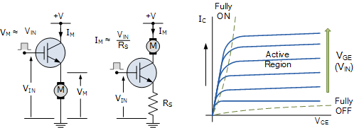
Image source: Electronics tutorials
From the figure above, current flows in one direction because IGBT is a unidirectional transistor.
Advantages of IGBT
The benefits of IGBT is mainly due to the combination of BJT and MOSFET into a single device. These benefits include:
- High power capabilities. They are designed to handle high voltage and current.
- Fast switching speed
- High input impedance
- Simple design hence easy to integrate into circuits
- Low input current losses since it is a voltage-controlled transistor
- Capable of switching high current using low voltage
- Has significantly high power gain
- High current density hence can fit into small devices but still deliver results
- Easy to switch ON and OFF
- Quite affordable than most alternatives
Disadvantages of IGBT
Despite the benefits, there are some cons of using Insulated Gate Bipolar Transistors. They include:
- Not able to block high reverse voltage
- More expensive than MOSFET and BJT
- Tend to have latching issues
- The transistors are unidirectional
Applications of IGBT
The most common application areas of IGBT include:
- Used in AC and DC motor drives where they control the speed of motors
- Used in AC inverters
- Used in sensitive medical equipment and devices
- Used in UPS systems
With this guide, you can proceed to buy IGBT in China for your needs. Whether you would want to use it on your project or would want to buy IGBT in bulk for wholesale, ensure you buy from reputable suppliers and distributors.
If you want to find more Electronic Components Distributors, please check out the following articles:
Electronic Components Distributors In the USA
Electronic Components Distributors In UK
Electronic Components Distributors In China
Electronic Components Distributors In India
Electronic Components Distributors In Singapore
Electronic Components Distributors In Malaysia
Electronic Components Distributors In Vietnam
Electronic Components Distributors In South Korea
- The Ultimate Guide to IRFZ44N MOSFET - April 30, 2024
- AMD Ryzen 5 vs Intel i5: How to Choose the Right Processor? - April 30, 2024
- Where to buy IC chips? The Best Guide? - March 26, 2024