Last Updated on October 23, 2023 by Kevin Chen
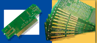
Image source Freepik
You may be wondering what is the relationship between fingers and PCB. To aggravate the situation, these fingers are made of gold. Yes, PCBs also have gold fingers, only that the fingers in this case have nothing to do with smuggling or carrying objects as many tend to assume. These fingers play an important role in the overall working, functionality, and performance of the printed circuit boards.
Are you planning to build PCBs from scratch? Or are you in the business of building printed circuit boards and would like to have valuable information about gold fingers? This is the perfect article for you. We are going to discuss in detail everything you should know about PCB gold fingers.
What are gold fingers?
Simply defined, gold fingers are gold-plated connectors that are embedded at the edges of the printed circuit boards. Since they are connectors, it means that their primary role is to connect different PCB components in order to complete electric circuits and at the same time execute various critical roles.
Since the gold fingers are placed at the edges of the printed circuit boards, they facilitate a perfect connection between the secondary components on the PCB to the main motherboard. PCB fingers are literally in every electronic device. You will find them in computers, laptops, and gaming consoles, among others. As long as a device will need a PCB, chances are it will have gold fingers.
Gold fingers in the electronic industry are always compared to the bridges in the real world. This is mainly because they provide links or connections for chips and other PCBs to interact with each other through various existing protocols. Some of these protocols are wired while others are wireless.
We can illustrate such a connection using a PCB that is embedded in a television and the other one on the remote controller. A TV is designed to receive and execute signals from the remote. Both the devices have PCB modules that make it possible to exchange data. Each PCB has gold fingers etched at the edges of the modules to facilitate the transfer and reception of data or electronic signals.
Why gold?
Why shouldn’t other materials be used on the fingers? It is easy to assume that gold plating aims to improve the aesthetics of the PCB fingers. After all, isn’t that one of the main functions of the gold plating?
Gold has desirable electric properties that make it an ideal platting for the PCB fingers. It is a good conductor of electricity hence allowing easy flow of electric current and signals in the PCB. Additionally, we cannot deny the malleability of the gold. It can easily adapt to different shapes and colors to fit on the printed circuit board.
The ability to resist corrosion and abrasion is another reason for using gold fingers. Since they are positioned at the edges of the printed circuit boards, they are easily exposed to external forces such as scratches and physical abrasion. Chemicals and other toxic elements can also corrode the PCB fingers. In addition to corrosion resistance, gold fingers have an even wear resistance.
It is also impossible to ignore the aesthetic value of using gold plating on the PCB fingers. Even as we focus on the core functionality of the fingers, we should appreciate the fact that gold plating is visually pleasing. They ensure that the PCB has a premium appearance, a factor that is likely to elevate its market value.
In short, the choice of gold plating on the PCB fingers wasn’t arrived at randomly. Engineers analyzed various properties of this material and the impact that it will have on the overall functionality and performance of the PCB.
Which gold is used on PCB gold fingers?
Two main types of gold are used for making PCB gold fingers. These are:
- Electroless Nickel Immersion Gold (ENIG): This type of gold is quite soft and thin hence making it easy to be soldered on the printed circuit board. It is also a cheaper option for making PCB gold fingers. However, the fact that it is soft makes it weak hence needs to be handled with extra precaution. For example, they are not ideal for frequent insertion and removal.
- Electroplated hard gold: Well, this is a thicker and denser gold material that is used for making PCB fingers. Its thickness can be as much as 30 micrometers. The thickness and high density of this material make it ideal for PCBs that are likely to be exposed to external forces such as corrosion and abrasion. They can wade off these risks.
Beyond the types, it is important to take note that gold plating the PCB fingers is an elaborate process that encompasses a series of steps. The ultimate goal is not just to plate but to ensure that the fingers acquire the desired reliability from the gold platting process. Keep in mind that the quality of work done during the platting process will determine the impact of the connections that you will make.
PCB fingers should undergo vigorous inspections both before and after the plating The surface on which the gold plating is applied should be free of impurities, dust, and dirt. You don’t want to encounter complications after you have already finished coating PCB fingers with gold. The sensitivity and relevance of this procedure are among the chief reasons why it is always put at the last stage of PCB manufacturing.
Using PCB gold fingers
Gold fingers are designed in a way that they can easily link or connect two PCB modules to achieve a streamlined integration. A strong and reliable connection should be created between the two printed circuits.
Individual properties of gold fingers will determine the strength and integrity of the connections that are created by the gold fingers. This is why it is important to know the types of gold that you are going to use on the gold fingers. For instance, hard gold is capable of withstanding harsh conditions. Also, it does not easily wear out or break no matter how many times it is mounted or dismounted.
Otherwise, there are three major ways of using PCB gold fingers. These are:
- Interconnection points: This mode of using the fingers entails using slots such as ISA and PCI to connect the fingers to the peripheral devices. These slots have gold fingers to allow strong and reliable connections. A perfect example is when you want to connect a memory slot to a motherboard. You will have to rely on the gold slots.
- Using external connectors: Gold fingers are also capable of implementing external connections with other PCBs and devices. This mode of using the fingers is usually ideal when you intend to facilitate the exchange of data between a computer and an external device. A USB cable or connector is a perfect example of such a connections. Other devices such as microphones and printers also use gold fingers to support such connections.
- Using specialized connectors: Beyond the general connections, manufacturers can build specialized PCB gold fingers for implementing specific connections. These PCBs are usually connected to specific sections of devices for optimized performance. A perfect example is the PCB gold fingers for graphics cards.
In all the three uses of PCB gold fingers that we have discussed, we have mainly focused on data or signal transfer between devices or different PCBs. But do you know that the fingers are also capable of supporting the transfer of electric signals between devices? PCB manufacturers ensure that the specifications of the gold fingers should support specific amounts of electric current and voltage. Like in all other conductors, current and voltage that exceed the limit of a conductor are likely to cause major damage.
Gold finger specifications
At this point, it is clear that you should not ignore the technical specifications of gold fingers. The specs will determine their suitability when etched on the PCB. A minor mistake or infraction is likely to affect the overall performance of the PCB. Wrong specifications are likely to result in a poor connection between the PCB and the gold fingers.
The IPC A-600 outlines several standards that PCB manufacturers should follow when manufacturing and assembling their printed circuit boards. Some of the gold finger specifications that are mentioned in the IPC include:
- Thickness: The thickness of the PCB gold finger should range between 2 to 50 microinches. The edges should be thicker than those of the prototypes
- The chemical composition of the gold fingers should be between 5% to 10% cobalt
- Visual and tape tests should be conducted on the PCB gold fingers.
PCB gold finger beveling
Beveling in the world of electronics refers to a process of shaving off the square corners of the fingers to form a slope. One of its goals is to enhance the physical and structural strength of the gold fingers when they are connected to other PCBs. PCB gold finger beveling also helps to secure connections between the gold fingers.
So, when buying a PCB in China, it is important to find out the type and specifications of the gold fingers that have been used. This information will be vital in determining the reliability of your PCB connections
If you want to find more Electronic Components Distributors, please check out the following articles:
Electronic Components Distributors In the USA
Electronic Components Distributors In UK
Electronic Components Distributors In China
Electronic Components Distributors In India
Electronic Components Distributors In Singapore
Electronic Components Distributors In Malaysia
Electronic Components Distributors In Vietnam
Electronic Components Distributors In South Korea
- The Ultimate Guide to IRFZ44N MOSFET - April 30, 2024
- AMD Ryzen 5 vs Intel i5: How to Choose the Right Processor? - April 30, 2024
- Where to buy IC chips? The Best Guide? - March 26, 2024