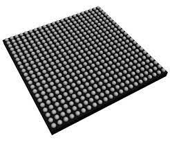
5CEFA5U19I7N
Part Number: 5CEFA5U19I7N
Manufacturer: Intel
Description: IC FPGA 224 I/O 484UBGA
Shipped from: Shenzhen/HK Warehouse
Stock Available: Check with us
ICRFQ.com - Electronic Components Distributor in China Since 2003

Part Number: 5CEFA5U19I7N
Manufacturer: Intel
Description: IC FPGA 224 I/O 484UBGA
Shipped from: Shenzhen/HK Warehouse
Stock Available: Check with us
| Datasheet | |
|---|---|
| Category | Integrated Circuits (ICs) |
| Family | Embedded – FPGAs (Field Programmable Gate Array) |
| Manufacturer | Altera |
| Series | Cyclone? V E |
| Part Status | Active |
| Number of LABs/CLBs | 29080 |
| Number of Logic Elements/Cells | 77000 |
| Total RAM Bits | 5001216 |
| Number of I/O | 224 |
| Number of Gates | – |
| Voltage – Supply | 1.07 V ~ 1.13 V |
| Mounting Type | Surface Mount |
| Operating Temperature | -40°C ~ 100°C (TJ) |
| Package / Case | 484-FBGA |
| Supplier Device Package | 484-UBGA (19×19) |
FPGAs, or Field Programmable Gate Arrays, are an important part of modern electronics. They offer flexibility and speed that can’t be beat. One FPGA that stands out is the 5CEFA5U19I7N Cyclone® V E FPGA IC, which is known for how well it works. It is used a lot in fields like telecommunications, industrial automation, the auto industry, and aircraft. In this guide, we’ll look at the 5CEFA5U19I7N FPGA’s architecture, features, tools, and uses, showing how much it can do for electronic designs. Come with us as we find out what this strong FPGA can do.
The 5CEFA5U19I7N FPGA is a high-performance FPGA that is part of the Cyclone® V-E family. It has a lot of great features and specs. Here are some of its most important traits:
The 5CEFA5U19I7N FPGA has a wide range of applications in a variety of industries, including:
Benefits and Advantages
The 5CEFA5U19I7N FPGA has a number of advantages that make it a favorite among designers:
The 5CEFA5U19I7N FPGA stands out because of its great features, many uses, and built-in benefits. Its high performance, flexibility, versatility, and energy efficiency make it a great choice for a wide range of electrical designs in fields like telecommunications, industrial automation, automotive, aerospace, medical, and defense.
The high performance of the 5CEFA5U19I7N FPGA is made possible by its flexible and powerful design. Let’s look at the internal parts and what they do to make things run smoothly:
These parts work well together to get jobs done quickly and efficiently in the FPGA. The logic elements carry out the logic functions and processes in the right order. The DSP blocks have specialized hardware resources for signal processing tasks that require a lot of computing power. The memory blocks store information in a way that makes it easy to access and get it back. The I/O parts make it easier to talk to devices and interfaces on the outside. Lastly, the clock control resources make sure that all of the timing in the FPGA design is correct.
Using the FPGA fabric’s ability to connect to other parts, designers can make complex designs by connecting these parts well. Because the FPGA can be programmed, these connections can be changed, and the design can be made better for certain jobs. The internal components and the programmable fabric work together to make the 5CEFA5U19I7N FPGA efficient, high-performing, and able to meet the needs of different uses.
In conclusion, the 5CEFA5U19I7N Cyclone® V E FPGA IC stands out as a high-performance and flexible option for a wide range of uses. It is the best choice for industries like telecommunications, industrial automation, automotive, aircraft, medical, and defense because of its impressive logic capacity, DSP blocks, and flexible I/O options.
The FPGA’s programmable nature enables rapid prototyping and system upgrades, while its internal components work seamlessly together to execute tasks efficiently. By embarking on an FPGA development journey and harnessing the power of the 5CEFA5U19I7N FPGA, you can unlock endless possibilities for innovation in your electronic designs. Order this exceptional product from ICRFQ, a leading electronic component distributor in China, and begin your FPGA journey to unleash your creative potential today.
WhatsApp us