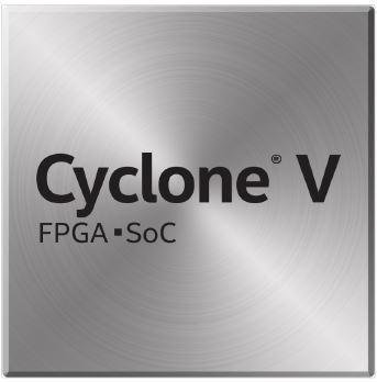
5CGXFC7C6F23I7N
Part Number: 5CGXFC7C6F23I7N
Manufacturer: Intel
Description: IC FPGA 240 I/O 484FBGA
Shipped from: Shenzhen/HK Warehouse
Stock Available: Check with us
ICRFQ.com - Electronic Components Distributor in China Since 2003

Part Number: 5CGXFC7C6F23I7N
Manufacturer: Intel
Description: IC FPGA 240 I/O 484FBGA
Shipped from: Shenzhen/HK Warehouse
Stock Available: Check with us
| Datasheet | |
|---|---|
| Category | Integrated Circuits (ICs) |
| Family | Embedded – FPGAs (Field Programmable Gate Array) |
| Manufacturer | Altera |
| Series | Cyclone? V GX |
| Part Status | Active |
| Number of LABs/CLBs | 56480 |
| Number of Logic Elements/Cells | 149500 |
| Total RAM Bits | 7880704 |
| Number of I/O | 240 |
| Number of Gates | – |
| Voltage – Supply | 1.07 V ~ 1.13 V |
| Mounting Type | Surface Mount |
| Operating Temperature | -40°C ~ 100°C (TJ) |
| Package / Case | 484-BGA |
| Supplier Device Package | 484-FBGA (23×23) |
FPGAs (Field Programmable Gate Arrays) have changed the way digital design and embedded systems work by giving them more flexibility and speed than ever before for a wide range of uses. The Cyclone® V GX stands out as a powerful and flexible solution among the top FPGA families. It can be used in a wide range of businesses and projects.
The Intel (formerly Altera) Cyclone® V GX family is a big step forward in FPGA technology. It gives designers a stable platform on which to apply complex digital designs, speed up algorithms, and build high-performance systems. It is a good choice for engineers and developers who want to push the limits of hardware creation because it has a unique set of features and abilities.
One of the most notable Cyclone® V GX models is the one with the number 5CGXFC7C6F23I7N. Let’s take a quick look at its main features:
The 5CGXFC7C6F23I7N FPGA comes in a Fine-Pitch Ball Grid Array (FBGA) package with 484 pins. The FBGA package has a high density of pins, which makes it easy to route data and makes it possible to make small circuit boards.
A semiconductor device called a Field Programmable Gate Array (FPGA) enables users to modify and change the hardware functionality of the device after it has been manufactured. FPGAs offer programmable logic and interconnect that may be tailored to implement different digital circuits, functions, and algorithms, in contrast to Application-Specific Integrated Circuits (ASICs), which are fixed and hardwired.
FPGAs are frequently used for digital design quick prototyping. They help engineers save time and money in the design process by allowing them to test and validate their hardware concepts before committing to ASIC fabrication.
FPGAs can be used to accelerate specific computationally-intensive tasks. By implementing FPGAs, which are specialized hardware accelerators, may carry out some tasks far more quickly than conventional CPUs, leading to notable performance advantages in niche applications like image processing, cryptography, and machine learning.
The ability to reconfigure FPGAs “on the fly” is one of its main benefits. This adaptability enables run-time dynamic adjustments as well as iterative design upgrades and requirement-driven adaptation. Applications, where the functionality needs to be frequently or remotely changed, can benefit the most from it.
Although the idea of programmable logic has been around since the 1960s, the first FPGA that was commercially available only appeared in the early 1980s. The first FPGA dubbed the XC2064, was released by Xilinx, which was established in 1984. Although it had a tiny capacity, it signaled the start of a new age in digital design.
FPGA technology advanced quickly during the 1980s and 1990s with the advent of bigger, more powerful devices. Additionally, new industry entrants like Altera (now a part of Intel) encouraged competition and innovation. FPGA architecture underwent substantial improvements in the early 2000s, allowing for more intricate designs and advanced degrees of integration.
FPGAs are currently pushing the limits of performance and capacity. To meet the needs of various applications, they add more sophisticated process nodes, better interconnect technologies, and specialized hardware blocks (such as DSP blocks and embedded memory) with each successive generation.
FPGAs are used in a variety of different industries, such as:
The basic components of an FPGA are called Configurable Logic Blocks (CLBs). Look-up tables (LUTs), which may implement any logic operation, flip-flops for data storage, and multiplexers for signal routing make up CLBs.
FPGAs differ from traditional CPUs and GPUs in their architecture and application domains:
The Cyclone® V GX family’s 5CGXFC7C6F23I7N FPGA features an advanced architecture with logic parts, embedded multipliers, and memory blocks for challenging digital designs. It offers plenty of resources for user designs, including RAM, DSP blocks, and PLLs. The FPGA’s capacity to be reconfigured allows for flexibility, adaptation to shifting demands, and hardware acceleration, but it also necessitates meticulous design verification and specialist knowledge. It provides a strong and adaptable overall solution for numerous digital design applications.
In conclusion, the 5CGXFC7C6F23I7N FPGA Cyclone® V GX family offers a powerful and versatile solution for modern digital design applications. With its abundance of resources and reconfigurability, it enables designers to create high-performance systems across various industries. Embrace the possibilities of FPGA technology, and explore its potential for innovation and hardware acceleration.
For those interested in obtaining the 5CGXFC7C6F23I7N FPGA at an affordable price, ICRFQ, a leading electronic component distributor in China, offers this remarkable FPGA model. Don’t miss the opportunity to harness the full potential of this cutting-edge technology with support from a trusted supplier.
WhatsApp us