L4960
Part Number: L4960
Manufacturer: STMicroelectronics
Description: Switching Voltage Regulators
Shipped from: Shenzhen/HK Warehouse
Stock Available: Check with us
ICRFQ.com - Electronic Components Distributor in China Since 2003

We make your sourcing easier!
Get A Fast Quote Worldwide!

Part Number: L4960
Manufacturer: STMicroelectronics
Description: Switching Voltage Regulators
Shipped from: Shenzhen/HK Warehouse
Stock Available: Check with us
| Datasheet | |
|---|---|
| Category | Integrated Circuits (ICs) |
| Family | PMIC – Voltage Regulators – DC DC Switching Regulators |
| Manufacturer | STMicroelectronics |
| Series | – |
| Packaging | Tube |
| Part Status | Active |
| Function | Step-Down |
| Output Configuration | Positive |
| Topology | Buck |
| Output Type | Adjustable |
| Number of Outputs | 1 |
| Voltage – Input (Min) | 9V |
| Voltage – Input (Max) | 46V |
| Voltage – Output (Min/Fixed) | 5.1V |
| Voltage – Output (Max) | 40V |
| Current – Output | 2.5A |
| Frequency – Switching | 100kHz ~ 150kHz |
| Synchronous Rectifier | No |
| Operating Temperature | -40°C ~ 150°C (TJ) |
| Mounting Type | Through Hole |
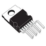
| Package / Case | Heptawatt-7 (Vertical, Bent and Staggered Leads) |
| Supplier Device Package | 7-HEPTAWATT |
The L4960 is a monolithic power switching regulator capable of delivering 2.5A at a voltage variable between 5V and 40V in step-down form. The device has various features, including current limitation, soft start, thermal protection, and a duty cycle of 0 to 100 percent for continuous operation mode. The L4960 is contained within a plastic power package rated at seven kilowatts and calls for an extremely limited number of additional components. Because of its efficient functioning at switching frequencies up to 150 kilohertz, the size and cost of the external filter components can be decreased.
| Input voltage | 50 | V | |
| V1 – V7 | Input to output voltage difference | 50 | V |
| V7 | Negative output DC voltage | -1 | V |
| Negative output peak voltage at t = 0.1µs; f = 100KHz | -5 | V | |
| V3, V5 | The voltage at pins 3 and 6 | 5.5 | V |
| V2 | The voltage at pin 2 | 7 | V |
| I3 | Pin 3 sink current | 1 | mA |
| I5 | Pin 5 source current | 20 | mA |
| Ptot | Power dissipation at Tcase ≤ 90°C | 15 | W |
| Tj, Tstg | Junction and storage temperature | -40 to 150 | °C |
A single chip or a controller can be used to build a switching regulator. Every one of the power switches—typically MOSFETs—is built into a single silicon chip in a monolithic switching regulator. For controllers, the positioning and selection of the power semiconductors are independent of the controller IC. Picking the right MOSFETs takes time and knowledge of the switch’s properties. When working with a monolithic design, designers avoid this problem altogether.
Also, the board area required by controller systems is typically larger than that required by fully integrated solutions. Consequently, it is not surprising that more and more switching regulators have been included in a single chip throughout the years, resulting in a wide variety of viable options for today, including those capable of handling greater power.
A controller solution offers greater flexibility, while monolithic solutions save room and are easier to design. A controller solution can have switches hand-picked by a designer that are optimized for the task at hand. The designer will also have access to the switches’ gates, allowing for the shrewd use of passive components to affect the switches’ switching edges. Furthermore, because large discrete switches can be selected and switching losses disappear with thermal isolation from the controller IC, controller systems are ideally suited for high power.
These are the advantages and disadvantages of a unified strategy that are brought up in conversation the most frequently; nevertheless, there is another perspective that should receive greater focus. Pay special attention to what is known as the “hot loops” if you wish to reduce the amount of radiated emissions produced by your switching regulator. Every switching regulator should strive for maximum EMC optimization as their end aim. As one of the key principles for accomplishing this goal, parasitic inductances in the applicable hot loop should be reduced to an acceptable level as much as possible. A buck converter’s “hot loop” includes the input capacitor, the high-side switch, the low-side switch, and the input capacitor. These paths that an electric current will take when its direction is rapidly reversed are extremely fast; the rapid changes in current result in a voltage offset, which couples into other portions of the circuit as interference via a parasitic inductance. This disrupts the normal operation of the circuit.
Although monolithic systems take up less space and have a simpler design process, the primary benefit of controller solutions is their increased degree of adaptability. A designer can select optimized and application-specific switches for a controller solution. Additionally, there is access to the gate for the switches, which makes it possible for the switching edges to be impacted by the creative use of passive components. In addition, controller solutions are appropriate for high power because large discrete switches can be chosen, and switching losses can be eliminated through thermal separation from the controller IC. This makes controller solutions suitable for applications that require a great deal of power.
On the other hand, in addition to these well-known reasons in favor of and against a monolithic solution, another facet is frequently neglected to be taken into consideration. The so-called “hot loops” in switching regulators are critical in achieving low radiated emissions. Every switching regulator should have its electromagnetic compatibility (EMC) improved as much as possible. One of the fundamental guidelines that must be adhered to achieve this goal is to reduce the amount of parasitic inductances present in each hot loop.
The term “hot loop” refers to the circuitry in a buck converter that includes the connection between the low-side switch and the input capacitor, the connection between the high-side switch and the low-side switch, and the connection between the high-side switch and the input capacitor. These are the paths in which the flow of a current change according to the rate at which the switching transitions take place.
Because of the fast variations in current, a voltage offset is created as a result of parasitic inductance. This voltage offset can then couple into other circuit segments as interference. Therefore, these parasitic inductances in the hot loops must be maintained at the lowest possible levels.
Thanks for reading. If you thought this post was interesting, feel free to look around the rest of our website for other content similar to what you just read. If you have any questions about the content of this article or any other article that can be found on our website, please feel free to leave them in the comment box below, and we will try our best to respond to them.
Contact us at ICRFQ, your leading electronic distributor of electronic components in china, if you would like more information or wish to purchase the L4960. We will ensure that you receive the best product at the best price possible.
WhatsApp us