ADA4096-2ACPZ
Part Number: ADA4096-2ACPZ
Manufacturer: Analog Devices Inc
Description: IC OPAMP GP 2 CIRCUIT 8LFCSP
Shipped from: Shenzhen/HK Warehouse
Stock Available: Check with us
ICRFQ.com - Electronic Components Distributor in China Since 2003

We make your sourcing easier!
Get A Fast Quote Worldwide!

Part Number: ADA4096-2ACPZ
Manufacturer: Analog Devices Inc
Description: IC OPAMP GP 2 CIRCUIT 8LFCSP
Shipped from: Shenzhen/HK Warehouse
Stock Available: Check with us
| Datasheet | |
|---|---|
| Category | Integrated Circuits (ICs) |
| Family | Linear – Amplifiers – Instrumentation, OP Amps, Buffer Amps |
| Manufacturer | Analog Devices Inc. |
| Series | – |
| Packaging | Tape & Reel (TR) |
| Part Status | Active |
| Amplifier Type | General Purpose |
| Number of Circuits | 2 |
| Output Type | Rail-to-Rail |
| Slew Rate | 0.4 V/μs |
| Gain Bandwidth Product | 786kHz |
| -3db Bandwidth | 1.52MHz |
| Current – Input Bias | 3nA |
| Voltage – Input Offset | 35μV |
| Current – Supply | 60μA |
| Current – Output / Channel | 10mA |
| Voltage – Supply, Single/Dual (±) | 3 V ~ 30 V, ±1.5 V ~ 15 V |
| Operating Temperature | -40°C ~ 125°C |
| Mounting Type | Surface Mount |
| Package / Case | 8-UFDFN Exposed Pad, CSP |
| Supplier Device Package | 6-LFCSP-UD (2×2) |
Rail-to-rail input and output ranges and micro power operation are two features of the ADA4096-2 dual and ADA4096-4 quad operational amplifiers. These amplifiers are ideal for monitoring battery utilization and managing battery charging due to their exceptionally low power requirements and guaranteed functioning between 3 V and 30 V.
They are recommended for battery-powered audio applications due to their dynamic performance, which includes a 27 nV/Hz voltage noise density. Without oscillation, capacitive loads up to 200 pF are handled. The ADA4096-2 and ADA4096-4 are the best devices for tough industrial applications because they contain overvoltage protection inputs and diodes that enable the voltage input to extend 32 V above and below the supply rails.
Overvoltage Protection, or OVP, is a feature of the ADA4096-2 and ADA4096-4 that enables the input voltage to safely exceed either supply without any phase reversal or latchup. The dual ADA4096-2 is offered in both 8-lead MSOP and 8-lead LFCSP (2 mm) packaging. The ADA4096-2 is offered in 14-lead TSSOP and 16-lead LFCSP (3 mm) packaging. The 8-lead MSOP package of the ADA4096-2W, which is approved for automotive applications, is available.
| EU RoHS | Compliant |
| ECCN (US) | EAR99 |
| Part Status | Active |
| HTS | 8542.33.00.01 |
| Automotive | No |
| PPAP | No |
| Type | Micropower Amplifier |
| Manufacturer Type | Micropower Amplifier |
| The Number of Channels per Chip | 2 |
| Rail to Rail | Rail to Rail Input/Output |
| The Maximum Input Offset Voltage (mV) | 0.3@±5V |
| The Minimum Single Supply Voltage (V) | 3 |
| The Typical Single Supply Voltage (V) | 5|9|12|15|18|24|28 |
| Maximum Single Supply Voltage (V) | 30 |
| The Minimum Dual Supply Voltage (V) | ±1.5 |
| The Typical Dual Supply Voltage (V) | ±3|±5|±9|±12 |
| The Maximum Dual Supply Voltage (V) | ±15 |
| Typical Low-Level Output Voltage (V) | -4.98 |
| Typical High-Level Output Voltage (V) | 4.97 |
| Maximum Input Offset Current (uA) | 0.002@±5V |
| Typical Input Bias Current (uA) | 0.01@±5V |
| Maximum Input Bias Current (uA) | 0.025@±5V |
| Maximum Supply Current (mA) | 0.11@±5V |
| Typical Output Resistance (Ohm) | 71 |
| Power Supply Type | Single|Dual |
| Typical Slew Rate (V/us) | 0.3@±5V |
| Typical Input Noise Voltage Density (nV/rtHz) | 27@±15V |
| Input Offset Voltage Drift (uV/°C) | 1(Typ) |
| Typical Voltage Gain (dB) | 111 |
| Typical Noninverting Input Current Noise Density (pA/rtHz) | 0.2@±5V |
| Minimum PSRR (dB) | 100 |
| Minimum CMRR (dB) | 72 |
| Minimum CMRR Range (dB) | 71 to 75 |
| Typical Gain Bandwidth Product (MHz) | 0.595 |
| Typical Settling Time (ns) | 23400 |
| Shut Down Support | No |
| Minimum Operating Temperature (°C) | -40 |
| Maximum Operating Temperature (°C) | 125 |
| Supplier Temperature Grade | Extended Industrial |
| Packaging | Tape and Reel |
| Mounting | Surface Mount |
| Package Height | 0.53 |
| Package Width | 2 |
| Package Length | 2 |
| PCB changed | 8 |
| Standard Package Name | CSP |
| Supplier Package | LFCSP EP |
| Pin Count | 8 |
| Lead Shape | No Lead |
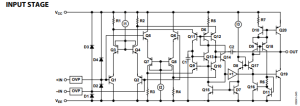
An ADA4096-2 schematic is shown in the figure above. Two differential pairs that function in parallel make up the input stage (Q1 to Q4 and Q5 to Q8). I1 reaches its lowest voltage compliance when the input common-mode voltage hits VCC 1.5 V, and Q1 to Q4 shut down. I2 reaches its minimal voltage compliance as Q5 to Q8 shut down when the input common-mode voltage approaches VEE + 1.5 V, on the other hand.
The amplifier can operate with its inputs at 200 mV outside the rail in this design, allowing for the widest input dynamic range possible (at room temperature). The CMRR of the amplifier is dependent on the VOS mismatch between the two input pairs, much like with any rail-to-rail input amplifier. Transitions between the input pairs are prevented if the input common-mode voltage range is maintained within 1.5 V of each rail, increasing the CMRR by around 10 dB.
When the input signal exceeds the amplifier’s common-mode voltage range, some single-supply amplifiers display phase inversion. The inverting and noninverting inputs exchange functions when the input devices are saturated. This causes the output to move oppositely.
Phase inversion can be harmful in situations where the amplifier is a part of a closed-loop system, even though it only lasts as long as the inputs are saturated.
The inputs of the ADA4096-2 series are guarded against input voltage excursions of up to 32 V outside each rail. This capability is especially crucial for situations where there may be problems with the order of the power supplies, which could result in the signal source turning on before the power supplies.
The figure below compares the ADA4096-2’s ability to limit input current (green curves) to using a 5 k series resistor.
The ADA4096-2 was used as a buffer, linking the supplies to GND (or 15 V) and scanning the positive input until it reached 32 V more than the supplies. Under conditions of positive overvoltage, the input current is typically restricted at 1 mA, and under conditions of negative Undervoltage, at 200 A. For example, the ADA4096-2 input current is limited to 1 mA at a 20 V overvoltage, providing a current limit similar to a series 20 k resistor. The above shows that the current limiting circuitry is active whether or not the amplifier is powered.
Op amps are very different from comparators, but a twin or quad op amp’s unused section can occasionally be utilized as a comparator. This is not advised for any op amps with rail-to-rail output, though. The output stage of rail-to-rail output operational amplifiers typically consists of a ratioed current mirror with bipolar or MOSFET transistors. The second stage increases the current drive to the ratioed mirror to close the loop while operating in an open lror. However, it is unable to do so, which causes a rise in supply current. The supply current can be much higher when the op-amp is set up as a comparator.
To meet the quality and dependability demands of automotive applications, the ADA4096-2W models are offered with controlled manufacturing. Designers should carefully read the Characteristics part of this data sheet as certain vehicle versions may have specifications that differ from the commercial models. The only products that can be used in automotive applications are those of automotive grade.
If you want more details or to buy the ADA4096-2ACPZ, contact us at ICRFQ, your go-to source for electronic components in China. We’ll make sure you get the greatest goods for the lowest price.
WhatsApp us