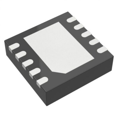
LTC2484IDD#TRPBF
Part Number: LTC2484IDD#TRPBF
Manufacturer: Analog Devices Inc.
Description: IC ADC 24BIT SIGMA-DELTA 10DFN
Shipped from: Shenzhen/HK Warehouse
Stock Available: Check with us
ICRFQ.com - Electronic Components Distributor in China Since 2003

Part Number: LTC2484IDD#TRPBF
Manufacturer: Analog Devices Inc.
Description: IC ADC 24BIT SIGMA-DELTA 10DFN
Shipped from: Shenzhen/HK Warehouse
Stock Available: Check with us
| Datasheet | |
|---|---|
| Category | Integrated Circuits (ICs) |
| Family | Data Acquisition – Analog to Digital Converters (ADC) |
| Manufacturer | Linear Technology |
| Series | – |
| Packaging | Tube |
| Part Status | Active |
| Number of Bits | 24 |
| Sampling Rate (Per Second) | 7.5 |
| Number of Inputs | 1 |
| Input Type | Differential |
| Data Interface | SPI |
| Configuration | MUX-ADC |
| Ratio – S/H:ADC | – |
| Number of A/D Converters | 1 |
| Architecture | Sigma-Delta |
| Reference Type | External |
| Voltage – Supply, Analog | 2.7 V ~ 5.5 V |
| Voltage – Supply, Digital | 2.7 V ~ 5.5 V |
| Features | Temperature Sensor |
| Operating Temperature | -40°C ~ 85°C |
| Package / Case | 10-WFDFN Exposed Pad |
| Supplier Device Package | 10-DFN (3×3) |
If you work in the analog-to-digital conversion industry, you’ve probably come across the LTC2484IDD#TRPBF. But what exactly is it, and why is it such an important participant in this field? In this in-depth look at the LTC2484IDD#TRPBF, we’ll look at its characteristics, capabilities, and applications.
The Linear Technology Corporation, now Analog Devices, LTC2484IDD#TRPBF is a cutting-edge analog-to-digital converter (ADC). This high-precision ADC combines a 24-bit No LatencyTM converter with patented EasyDriveTM technology, making it an exceptional solution for a variety of applications.
The Linear Technology Corporation (now Analog Devices) LTC2484IDD#TRPBF is a small 24-bit analog-to-digital converter (ADC) with amazing characteristics. In this quick overview, we’ll look at the unique features that make it a must-have tool for engineers and designers.
In conclusion, the LTC2484IDD#TRPBF is a flexible ADC with advanced capabilities, exceptional accuracy, and adaptability. This device has the potential to improve your designs whether you’re working on precision instruments, sensor data acquisition, or any other application that requires high-performance analog-to-digital conversion. Its small size and ease of integration make it a great asset for engineers and designers striving for data collecting excellence.
The remarkable feature set of the LTC2484IDD#TRPBF makes it a versatile solution for a variety of applications:
The LTC2484IDD#TRPBF’s 24-bit resolution and EasyDriveTM technology provide the accuracy and reliability necessary in applications requiring high-precision measurements, such as scientific instruments and test equipment.
The LTC2484IDD#TRPBF can deliver exact analog signal conversion even in electrically noisy situations for industrial automation systems that require accurate monitoring and control of processes.
The LTC2484IDD#TRPBF’s low latency and strong line frequency rejection characteristics ensure that data obtained is both accurate and dependable in sensor-based applications such as environmental monitoring or healthcare devices.
This ADC can handle a wide common mode input range and line frequency rejection in energy management and power metering systems, making it appropriate for applications such as smart grid monitoring.
The LTC2484 is a low-power delta-sigma analog-to-digital converter with a simple 4-wire serial interface and automated differential input current cancellation. Let us investigate its operation and some of its practical applications.
The LTC2484 runs in three distinct states during the course of its operating cycle:
When the CS pin is pulled LOW, the device leaves low-power mode and enters the data output state. If CS is set to HIGH before the first rising edge of the serial clock (SCK), the device enters low-power sleep mode, and the conversion result is stored in the internal static shift register. If CS remains LOW after the initial rising edge of SCK, however, the device begins to output the conversion result. Raise CS at this moment to end the data input and output states and start a fresh conversion. On the falling edge of SCK, the conversion result is moved out through the serial data output pin (SDO).
The LTC2484’s 4-wire serial interface simplifies communication and control. It consists of the following components:
In conclusion, the LTC2484IDD#TRPBF stands as a testament to modern analog-to-digital conversion technology, offering a remarkable blend of adaptability, precision, and advanced features. Its capabilities have the power to elevate your design projects, whether they involve crafting precision instruments, acquiring sensor data, or any application demanding top-tier analog-to-digital conversion performance.
To unlock the potential of this cutting-edge device, ICRFQ, a renowned electronic component distributor in China, offers it at an affordable price. By securing your LTC2484IDD#TRPBF through ICRFQ, you ensure access to the forefront of technological innovation. Don’t miss the opportunity to take your projects to the next level with this exceptional ADC.
WhatsApp us