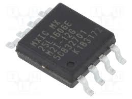
MX25L1606EM2I-12G
Part Number: MX25L1606EM2I-12G
Manufacturer: Macronix
Description: IC FLASH 16MBIT SPI 86MHZ 8SOP
Shipped from: Shenzhen/HK Warehouse
Stock Available: Check with us
ICRFQ.com - Electronic Components Distributor in China Since 2003

Part Number: MX25L1606EM2I-12G
Manufacturer: Macronix
Description: IC FLASH 16MBIT SPI 86MHZ 8SOP
Shipped from: Shenzhen/HK Warehouse
Stock Available: Check with us
| Datasheet | |
|---|---|
| Category | Integrated Circuits (ICs) |
| Family | Memory |
| Manufacturer | Macronix |
| Series | MX25xxx05/06 |
| Packaging | Tube |
| Part Status | Active |
| Format – Memory | FLASH |
| Memory Type | FLASH – NOR |
| Memory Size | 16M (2M x 8) |
| Speed | 86MHz |
| Interface | SPI Serial |
| Voltage – Supply | 2.7 V ~ 3.6 V |
| Operating Temperature | -40°C ~ 85°C (TA) |
| Package / Case | 8-SOIC (0.209″, 5.30mm Width) |
| Supplier Device Package | 8-SOP |
The MX25L1606EM2I-12G is a Flash NOR memory IC with a maximum speed of 86 MHz and the ability to store 16 megabits (2 megabytes). It is used in many electronic products that need non-volatile storage because it is small and has an SPI interface. This detailed guide is meant to give you an overview of the MX25L1606EM2I-12G by describing its most important features, specifications, and typical uses.
Macronix makes the MX25L1606EM2I-12G. It is a Flash NOR memory IC. It is made to let a wide range of electronic gadgets store information that doesn’t change when the power goes out. With 16 megabits (2 megabytes) of storage space, it is a reliable and efficient way to store computer code, configuration data, and other important data.
The Serial Peripheral Interface (SPI) is used by the MX25L1606EM2I-12G to talk to the main microcontroller or system. Since many microcontrollers and other devices support the SPI interface, this makes it easy to add to different apps.
The MX25L1606EM2I-12G has a number of important features that make it a good choice for a wide range of memory storage needs. Some of the things that stand out are:
The IC has a storage capacity of 16 megabits, which is equal to 2 megabytes. This makes it possible to store a lot of data, such as computer code, configuration settings, and other important data.
The famous Serial Peripheral Interface (SPI) is used to talk to the MX25L1606EM2I-12G. The SPI interface makes it easy to connect microcontrollers and other devices and send data quickly.
It has a maximum working frequency of 86 MHz, which means it can read and write data quickly and efficiently.
The IC is made to work with little power, so it can be used in battery-powered devices or uses that have strict power needs.
The MX25L1606EM2I-12G works successfully in a wide range of temperatures, usually from -40°C to +85°C, so it can be used in a variety of places and situations.
The IC comes in an 8-SOP (Small Outline box), which is a small and common box type that makes it easy to add to different circuit designs.
Both byte and page write tasks can be done on the MX25L1606EM2I-12G, so data can be written to specific memory locations. Here is a broad description of the write operation:
To delete data from memory, the MX25L1606EM2I-12G offers chip or sector wipe operations. Larger blocks of erasure are used to maximize efficiency. The following are the erase operations:
Several security features are built into the MX25L1606EM2I-12G to protect data integrity and stop unintentional changes. Among these mechanisms are:
Write operations to the memory can be stopped, protecting it from unintentional writes, by holding the /WP pin at a low voltage. The host controller or system can manage write protection by controlling this pin.
The device may offer software-based write protection methods that allow for the read-only designation of particular memory sectors or regions. Usually, this protection is managed by means of a set of commands or configuration registers.
Lock Bits: Some MX25L1606EM2I-12G variations may have lock bits that can be configured to permanently shield some memory areas from editing or erasing. A higher level of data security is provided by the inability to modify or erase these zones once they have been locked.
The individual commands, addresses, and protection measures offered by the MX25L1606EM2I-12G should be thoroughly reviewed in the device datasheet because they may change based on the precise device model.
Experience reliable and efficient non-volatile storage with the MX25L1606EM2I-12G Flash NOR memory IC. It offers capacity, speed, and interface compatibility for diverse applications. With low power consumption, a wide temperature range, and built-in protection mechanisms, it adapts to any environment. Unlock your project’s potential—order the MX25L1606EM2I-12G from ICRFQ today.
WhatsApp us