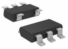
SN74LVC1G07DCKR
Part Number: SN74LVC1G07DCKR
Manufacturer: Texas Instruments
Description: IC BUF NON-INVERT 5.5V SC70-5
Shipped from: Shenzhen/HK Warehouse
Stock Available: Check with us
ICRFQ.com - Electronic Components Distributor in China Since 2003

Part Number: SN74LVC1G07DCKR
Manufacturer: Texas Instruments
Description: IC BUF NON-INVERT 5.5V SC70-5
Shipped from: Shenzhen/HK Warehouse
Stock Available: Check with us
| Datasheet | |
|---|---|
| Category | Integrated Circuits (ICs) |
| Family | Logic – Buffers, Drivers, Receivers, Transceivers |
| Manufacturer | Texas Instruments |
| Series | 74LVC |
| Packaging | Tape & Reel (TR) |
| Part Status | Active |
| Logic Type | Buffer, Non-Inverting |
| Number of Elements | 1 |
| Number of Bits per Element | 1 |
| Input Type | – |
| Output Type | Open Drain |
| Current – Output High, Low | -, 32mA |
| Voltage – Supply | 1.65 V ~ 5.5 V |
| Operating Temperature | -40°C ~ 125°C (TA) |
| Mounting Type | Surface Mount |
| Package / Case | 5-TSSOP, SC-70-5, SOT-353 |
| Supplier Device Package | SC-70-5 |
Texas Instruments has made the SN74LVC1G07DCKR buffer and line driver, which is the best way to boost digital and analog signals and connect the input to a transmission line. This powerful part has an open drain output, meaning your project will have the best power management. This non-inverting device is adaptable and dependable, with a temperature range of -40 °C to 125 °C and only one channel per chip, making it the ideal option for various applications. The SN74LVC1G07DCKR will also be shipped in a tape-and-reel package, making it safe to ship and easy to install. This line driver is a reliable and efficient choice for your next project. Normal operating supply voltages are 1.8, 2.5, 3.3, or 5 V. The minimum operating supply voltage is 1.65 V.
This single buffer/driver is intended for use with VCC voltages ranging from 1.65 V to 5.5 V. It is possible to build active-low wired-OR or active-high wiredAND functionality by connecting the open drain output of the SN74LVC1G07 device to other open-drain outputs to create a network. The SN74LVC1G07 output is an open drain. The sink current can reach a maximum of 32 mA. The SN74LVC1G07 can be purchased in several different packages, one of which is the incredibly compact DPW packaging, which has a body that measures 0.8 millimetres on the side.
In short, the SN74LVC1G07DCKR buffer and line driver from Texas Instruments is a reliable and flexible part that manages power well and works well. It can be used in many electronic projects because it has an open-drain output, a polarity that doesn’t flip, and a wide temperature range. This part is easy to install and safe to ship because it comes on a tape and reel and is mounted on a surface.
The SN74LVC1G07 component has one open-drain buffer and a maximum sink current of 32 milliamperes (mA). This device fulfils all requirements for partial-power-down applications that make use of Ioff. When the device is turned down, the Ioff circuitry turns off the outputs, which stops potentially harmful currents from flowing backwards through the device. In integrated circuit packaging, the DPW package technology represents a significant step forward. Compared to other package alternatives, the DPW 0.64 mm square footprint takes up significantly less area on the circuit board while maintaining the conventionally manufacturing-friendly lead pitch of 0.5 mm.
It is possible to create a high-output drive buffer with the help of the high-drive CMOS device known as the SN74LVC1G07, which is suitable for LED applications. As a result of its ability to sink 32 mA of current at 4.5 V, it is ideally suited for high drive and wired-OR/AND operations. It works well for high-speed applications with a maximum frequency of 100 MHz. The inputs can tolerate up to 5.5 V, translating up or down to VCC.
This device utilizes Design Requirements CMOS technology, featuring a balanced output drive. Bus contention should be avoided at all costs since it can generate currents higher than the maximum allowed levels. The high drive will also cause quick edges into mild loads, so it is important to consider the routing and load conditions to avoid ringing.
Inputs should never be allowed to float while working with multiple-bit logic devices. In many applications, digital logic device functionalities or portions of functions are not being utilized. This might happen, for instance, when only two of a triple-input AND gate’s three inputs are being used or when only three of a buffer gate’s four inputs are being used. Because the uncertain voltages at the outside connections can result in undefined operating states, such input pins should never be disconnected. To stop them from floating, When digital logic devices are not being used, their unused inputs must all be wired to either a high or low bias. It depends on the device’s purpose to determine the logic level that should be assigned to any unused input. In most cases, they will be connected to GND or Vcc, depending on which source provides easier access.
In conclusion, the Texas Instruments SN74LVC1G07DCKR buffer and line driver is a powerful and flexible part that can easily boost digital and analog signals. This device is great for many uses because it has an open drain output and efficiently manages power. It works well and is reliable because it can work from -40°C to 125°C and has only one channel per chip. Also, the tape and reel packaging ensures it arrives safely and can be mounted well. As a leading electronic distributor in China, ICRFQ offers this impressive device. Please contact us today to learn how it can help your next project.
WhatsApp us