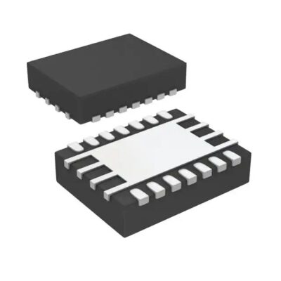
TPS63020DSJR
Part Number: TPS63020DSJR
Manufacturer: Texas Instruments
Description: IC REG BCK BST ADJ 3.5A 14VSON
Shipped from: Shenzhen/HK Warehouse
Stock Available: Check with us
ICRFQ.com - Electronic Components Distributor in China Since 2003

Part Number: TPS63020DSJR
Manufacturer: Texas Instruments
Description: IC REG BCK BST ADJ 3.5A 14VSON
Shipped from: Shenzhen/HK Warehouse
Stock Available: Check with us
| Datasheet | |
|---|---|
| Category | Integrated Circuits (ICs) |
| Family | PMIC – Voltage Regulators – DC DC Switching Regulators |
| Manufacturer | Texas Instruments |
| Series | – |
| Packaging | Tape & Reel (TR) |
| Part Status | Active |
| Function | Step-Up/Step-Down |
| Output Configuration | Positive |
| Topology | Buck-Boost |
| Output Type | Adjustable |
| Number of Outputs | 1 |
| Voltage – Input (Min) | 1.8V |
| Voltage – Input (Max) | 5.5V |
| Voltage – Output (Min/Fixed) | 1.2V |
| Voltage – Output (Max) | 5.5V |
| Current – Output | 3.5A (Switch) |
| Frequency – Switching | 2.4MHz |
| Synchronous Rectifier | Yes |
| Operating Temperature | -40°C ~ 85°C (TA) |
| Mounting Type | Surface Mount |
| Package / Case | 14-VFDFN Exposed Pad |
| Supplier Device Package | 14-VSON (4×3) |
An adjustable positive output voltage of up to 3.5A can be provided by the potent Buck-Boost Switching Regulator IC known as the TPS63020DSJR. This IC, protected by a 14-VFDFN exposed pad package, provides great efficiency and flexibility in power management for various applications. The TPS63020DSJR can be the perfect choice if you seek a dependable answer to your power management demands.
The device’s control circuit is built using an average current mode topology. Additionally, input and output voltage feed-forward is used by the controller. The duty cycle of the modulator can be changed promptly to achieve a quick response to such faults when changes in input and output voltage are detected. The FB pin serves as the feedback input for the voltage error amplifier. A resistive voltage divider must be attached to that pin for variable output voltages. FB must be linked to the output voltage to directly sense the voltage at fixed output voltages. Versions with fixed output voltage employ an internally trimmed resistive divider. The feedback voltage will be compared to the internal reference voltage to produce a steady and precise output voltage.
The device incorporates four internal N-channel MOSFETs to maintain synchronous power conversion under all conceivable operating situations. As a result, the device can maintain high efficiency over a wide range of input voltage and output power. Two distinct ground pins, GND and PGND, are employed to prevent ground shift issues from the high currents in the switches. The GND pin serves as the reference for all control operations. To PGND are connected the power switches. On the PCB, ideally adjacent to the GND pin, one location must be linked to both grounds. The load is always removed from the input during converter shutdown due to the 4-switch structure. A temperature sensor is installed to prevent the device from overheating.
An inbuilt limit on the average inductor current, which stays constant under ideal operating conditions, protects the component and the application. The current limit is, however, reduced if the voltage provided at VIN falls below 2.3 V. This may occur when the battery capacity is nearly exhausted, the output impedance rises, or the battery is subjected to a heavy pulse load, all of which lower VIN voltage. The dynamic current limit is at its lowest point when the minimum acceptable VIN supply voltage is reached. The gadget must run in burst mode at this voltage to maintain operation despite a poor input power source.
A built-in power-good feature on the gadget lets you know whether or not the output voltage is correctly regulated. The average inductor current limit causes the power-good output to become low impedance as soon as it is achieved. If not required, the open-drain output can be left open. The supply voltage of the externally attached logic can be changed to remain within the absolute maximum ratings by connecting a pullup resistor to it. The power-good output gives the connected application the most time to safely respond to an output voltage breakdown since it keeps an eye on the state of the current control loop.
Control of the output voltage will cease to function if, for whatever reason, the output voltage is not properly sent back to the voltage amplifier’s input. Overvoltage protection is provided to prevent the output voltage from reaching critical values for the device and potentially for the system it is powering. The overvoltage protection circuit also monitors the internal output voltage in place. The voltage amplifier adjusts the output voltage to this level in the event that it crosses the overvoltage threshold.
The TPS63020DSJR can be used in renewable energy systems like solar and wind power. It’s a great option for these applications since it can efficiently manage power from these sources and transform it into useful energy.
The TPS63020DSJR Buck-Boost Switching Regulator IC is a powerful and versatile answer for power management needs in several applications, including battery-powered devices, IoT devices, industrial automation, automotive, power banks, aerospace and defense, and renewable energy systems. Due to its adjustable output voltage, excellent efficiency, and various working modes, this IC offers exceptional flexibility and dependability for enhancing power management. Built-in features that enhance the linked system’s functionality and safety include a power good, dynamic current limit, and overvoltage protection.
If you’re looking for a dependable and efficient way to meet your power management needs, the TPS63020DSJR might be a wonderful choice. If you’re looking to buy a MOSFET or other electronic component, ICRFQ also has a sizable selection of parts.
WhatsApp us