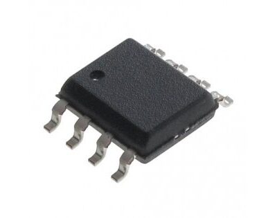
W25Q128JVSIQ
Part Number: W25Q128JVSIQ
Manufacturer: Winbond Electronics
Description: IC FLASH 128MBIT SPI/QUAD 8SOIC
Shipped from: Shenzhen/HK Warehouse
Stock Available: Check with us
ICRFQ.com - Electronic Components Distributor in China Since 2003

Part Number: W25Q128JVSIQ
Manufacturer: Winbond Electronics
Description: IC FLASH 128MBIT SPI/QUAD 8SOIC
Shipped from: Shenzhen/HK Warehouse
Stock Available: Check with us
| Category | Integrated Circuits (ICs) |
|---|---|
| Family | Memory |
| Manufacturer | Winbond Electronics |
| Series | SpiFlash? |
| Packaging | Tray |
| Part Status | Active |
| Format – Memory | FLASH |
| Memory Type | FLASH – NOR |
| Memory Size | 128M (16M x 8) |
| Speed | 104MHz |
| Interface | SPI Serial |
| Voltage – Supply | 2.7 V ~ 3.6 V |
| Operating Temperature | -40°C ~ 85°C (TA) |
| Package / Case | 8-SOIC (0.209″, 5.30mm Width) |
| Supplier Device Package | 8-SOIC |
The W25Q128JV Serial Flash memory offers a dependable, high-performance application storage solution. The W25Q128JV, part of the 25Q family, offers better performance and customizability than traditional Serial Flash media. In addition to storing voice, text, and data, this design is also well suited for code shadowing to RAM and direct code execution through Dual/Quad SPI (XIP). When powered off, the W25Q128JV runs on a 2.7V to 3.6V supply and uses under 1uA of electricity.
The W25Q128JV is ideal for settings with limited storage capacity because of its tiny form factor. 65,536 programmable pages of 256 bytes each comprise its memory array, which may edit up to 256 simultaneously. Thanks to the 4,096 erasable sectors and 256 erasable blocks given by the tiny 4KB sectors, the chip can be erased in 32KB block erase, 64KB block erase, or chip erase in 16-page chunks, 128-page chunks, 256-page chunks, or all at once. As a result, developers have more creative freedom when creating programs that store data and parameters.
The Serial Peripheral Interface (SPI) peripherals Serial Clock, Dual/Quad I/O SPI, Chip Select, and Serial Data I/O1 (DO), I/O0 (DI), I/O2, and I/O3 are all compatible with the W25Q128JV. It is possible to attain clock speeds using Fast Read Dual/Quad I/O comparable to those of traditional Asynchronous 8-bit and 16-bit Parallel Flash memory, namely 266MHz (532MHz (133MHz x 4) for Quad I/O and 133MHz x 2) for Dual I/O.
In addition to its three 256-byte Security Registers and 64-bit Unique Serial Number, the W25Q128JV also supports SFDP and the JEDEC standard for manufacturer and device ID. Thanks to these qualities, the gadget is a safe and dependable solution for various applications.
Overall, the W25Q128JV Serial Flash memory exceeds traditional Serial Flash devices in a number of crucial areas, making it a cutting-edge and adaptable storage solution. It is a great option for high-performance and dependable memory storage applications due to its low power consumption, small size, support for various erase sectors, and multiple clock speeds.
The SPI-compatible bus, which consists of the four signals Serial Clock and Serial Data Output (DO), is designed to make it simple to access the W25Q128JV Serial Flash memory. With Standard SPI instructions, the DI input pin on the rising edge of CLK can be used to write instructions, addresses, or data to the device. On the falling edge of CLK, the DO output pin is utilized to receive data or status from the device.
The device can operate the SPI bus in Modes 0 (0,0) and 3 (1,1). The typical status of the CLK signal while the SPI bus master is on standby and no data is being sent is the main distinction between Mode 0 and Mode 3. While the CLK signal in Mode 3 is often high on both the falling and rising edges, it is typically low on both edges in Mode 0.
The W25Q128JV features Dual SPI operation, which is accessed by means of particular instructions. Compared to standard Serial Flash devices, this capability offers an impressively two to three times faster data transfer rate. Dual SPI Read instructions are ideal for downloading non-speed critical code directly from the SPI bus (XIP) or code-shadowing during power-up. The DI and DO pins become IO0 and IO1 bidirectional I/O pins using Dual SPI instructions.
The W25Q128JV flash memory device uses instructions like “Fast Read Quad Output (6Bh)” and “Fast Read Quad I/O (EBh)” to enable Quad SPI operation. The data transmission rates made possible by these instructions are four to six times faster than those made possible by conventional Serial Flash memory devices. The DI and DO pins are changed into the bidirectional IO0 and IO1 pins by using Quad SPI instructions, and two extra I/O pins, IO2 and IO3, become usable.
In conclusion, the W25Q128JV Serial Flash memory, which offers cutting-edge features like adjustable erase sectors, clock frequencies, and security settings, is a superb solution for high-performance and dependable memory storage needs. It is the perfect solution for code shadowing, running code directly from Dual or Quad SPI, and storing voice, text, and data since it can enable real XIP operation and support various applications.
Contact ICRFQ, your reliable electronic component supplier, if you want to order the W25Q128JV or find out more about its features. Don’t wait to get in touch with them right away to benefit from this innovative technology!
WhatsApp us